
Process independent curvature compensation scheme for bandgap reference

a bandgap reference and compensation scheme technology, applied in the direction of electric variable regulation, process and machine control, instruments, etc., can solve the problems of limiting the temperature drift performance of such a reference, affecting the accuracy of reference voltages, and reducing the dynamic range of reference voltages, so as to improve the regulation capability

Active Publication Date: 2009-12-22
ELITE SEMICON MEMORY TECH INC
View PDF6 Cites 16 Cited by
  • Summary
  • Abstract
  • Description
  • Claims
  • Application Information

AI Technical Summary

Benefits of technology

The solution provides a high-precision, trim-free bandgap circuit with improved temperature stability, reducing temperature drift and making the circuit applicable to standard CMOS processes while simplifying layout and process matching.

Problems solved by technology

Unfortunately, lower dynamic range (a consequence of low voltage) demands that reference voltages be more accurate.
In particular, the bandgap reference generates a strong second-order term that varies with T ln(T), and which limits the temperature drift performance of such a reference, i.e., causes deviation of the reference voltage with temperature.
While these second order terms may be relatively small, their impact can prove highly undesirable for many applications.
While these methods may be utilized with some success, limitations exist over process availability and process variations.
Most notably, many of these methods have been configured to address applications utilizing bipolar transistors, but can not be utilized effectively with CMOS applications.
This limitation of prior art methods results from that the parasitic vertical bipolar transistor available in standard CMOS process has its collector always connected to substrate and limits the use of vertical bipolar transistor as an emitter follower.
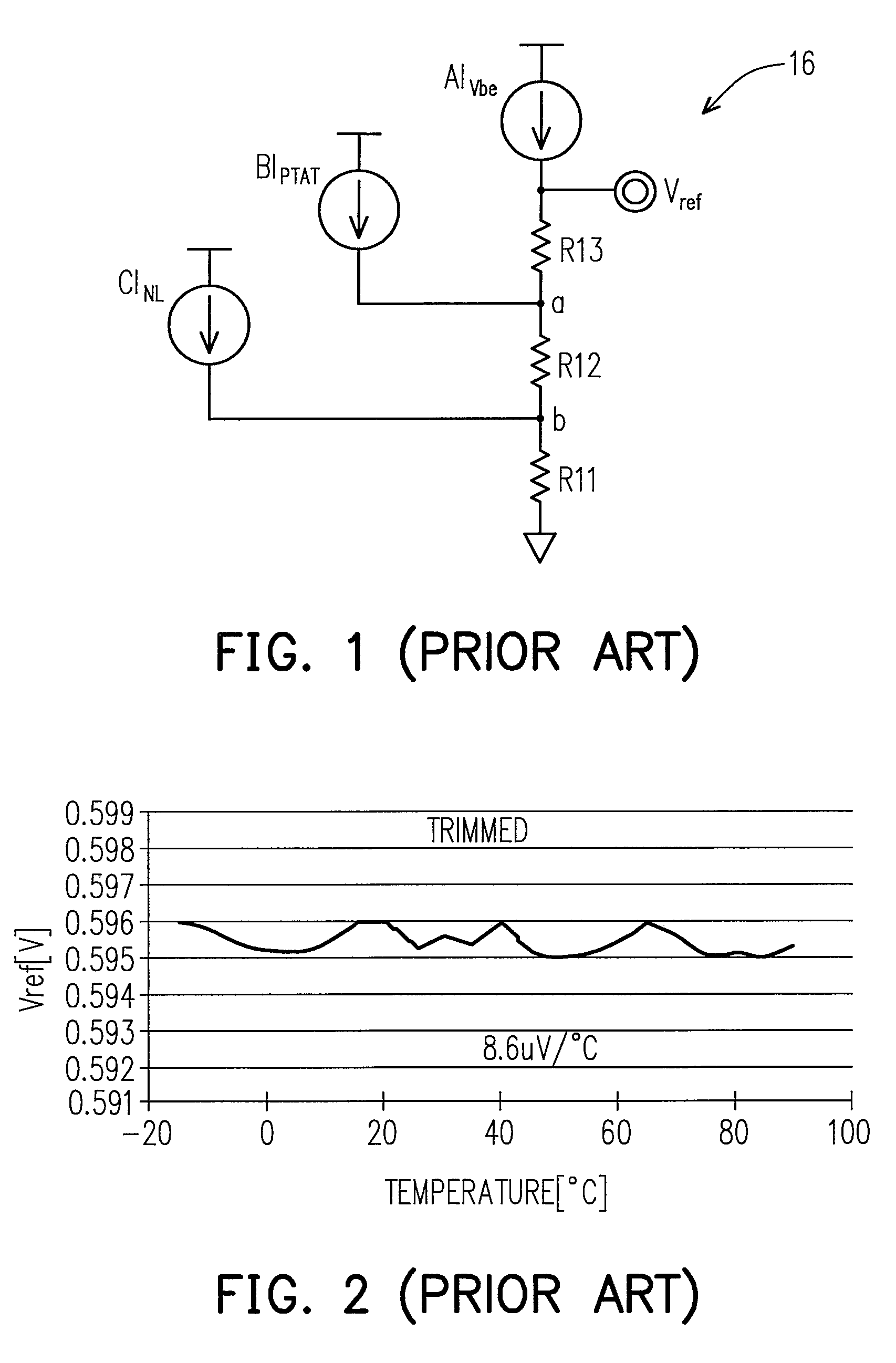
However, actually, INL just moves in the opposite way and worsens offset of the bandgap reference voltage.
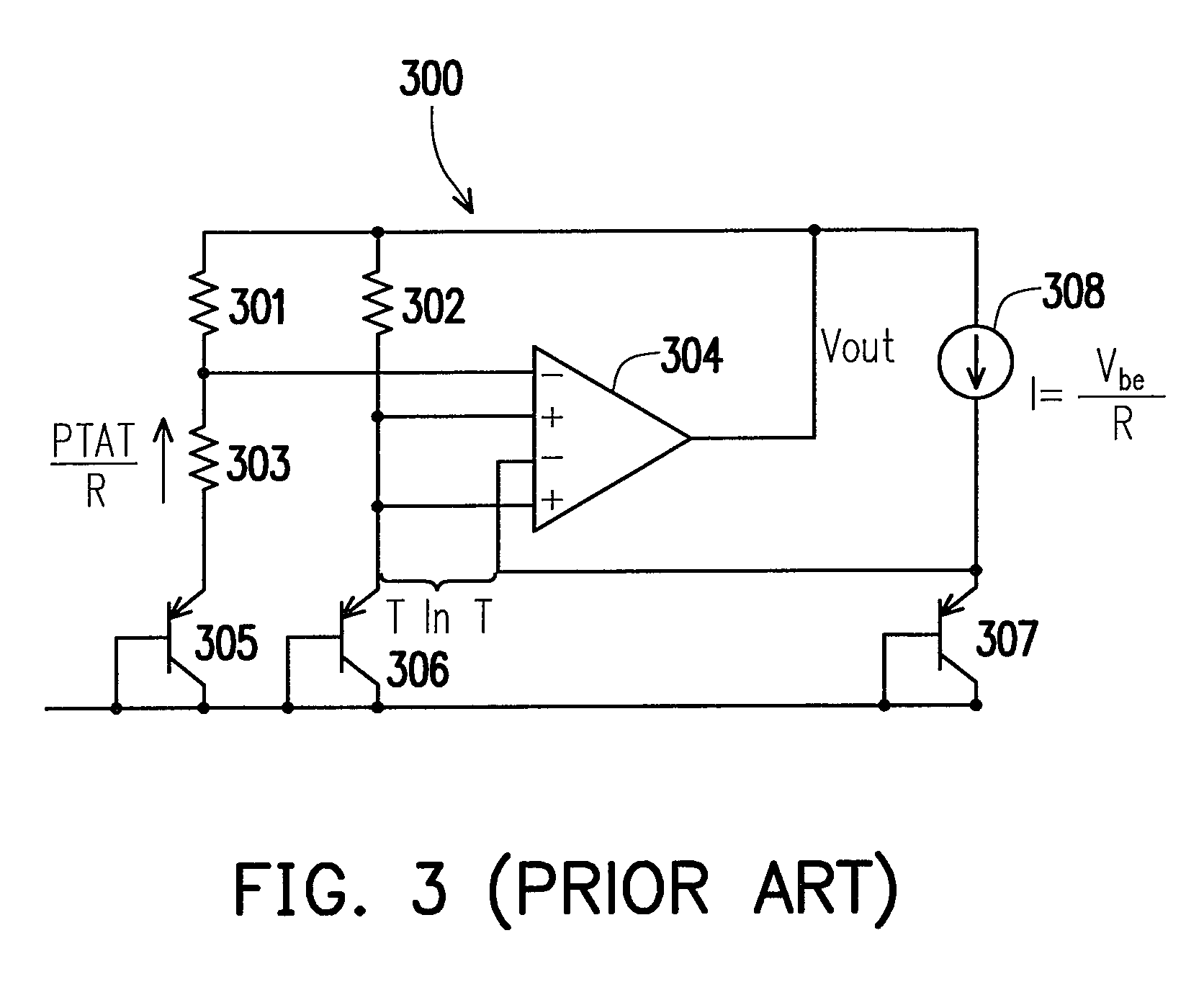
However, too many BJT transistors are used to implement the architecture of FIG. 3 and accordingly matching between BJT transistors is poor.
So, curvature compensation effect provided by the architecture of FIG. 3 is process sensitive, which is undesirable.
Further, as for the dual differential pairs in the OP 304, 4 PMOS transistors have to be matched well, which is difficult because each pair has its own N-well.

Method used


Image

  • Process independent curvature compensation scheme for bandgap reference
  • Process independent curvature compensation scheme for bandgap reference
  • Process independent curvature compensation scheme for bandgap reference

Examples


first embodiment

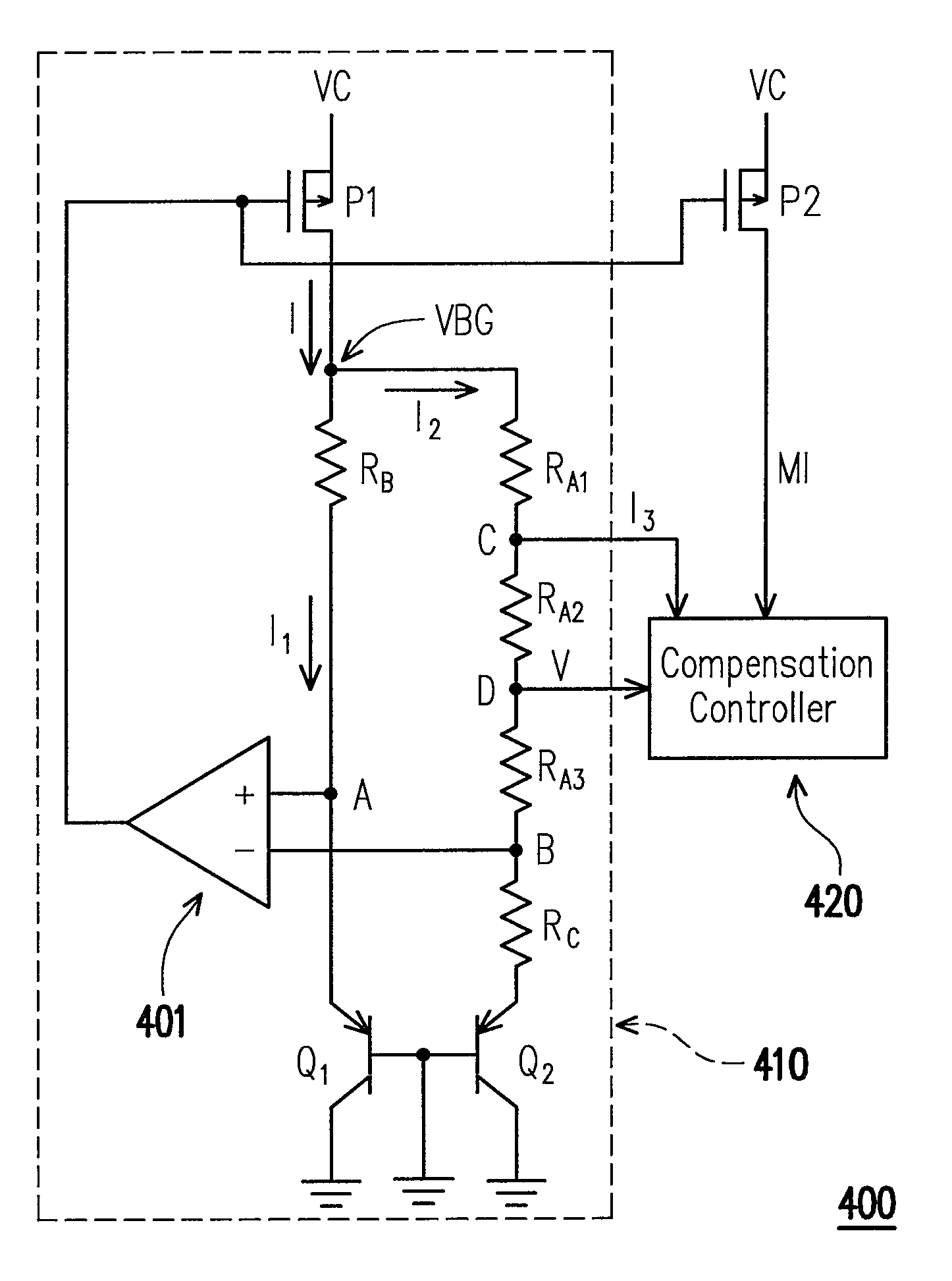
[0038]FIG. 4 shows a voltage reference circuit according to a first embodiment of the invention. As shown in FIG. 4, the voltage reference circuit 400 includes: a bandgap reference circuit 410, a compensation controller 420 and a PMOS transistor P2. The bandgap reference circuit 410 is for generating a bandgap reference voltage VBG and a reference current I. The compensation controller 420 is coupled to the bandgap reference circuit 410 and the transistor P2. The compensation controller 420 converts a node voltage V at node D into a current N1Ic and performs current subtraction on the current MI (from the transistor P2) and the current N1Ic to provide a compensation feedback current I3 to node C of the bandgap reference circuit 410. So that, the bandgap reference voltage VBG is temperature compensated.

[0039]The bandgap reference circuit 410 includes: an operation amplifier 401, a PMOS transistor P1, BJT transistors Q1 and Q2, and resistors RA1, RA2, RA3, RB and Rc. Resistors RA1, RA...

second embodiment

[0069]FIG. 8 shows a voltage reference circuit according to a second embodiment of the invention. As shown in FIG. 8, the voltage reference circuit 800 includes: a bandgap reference circuit 810, a compensation controller 820, a current inverter 830 and a PMOS transistor P2. The bandgap reference circuit 810, the compensation controller 820 and the PMOS transistor P2 in the second embodiment may be similar or the same as the bandgap reference circuit 410, the compensation controller 420 and the PMOS transistor P2 in the first embodiment and accordingly the details thereof are omitted here.

[0070]In the bandgap reference circuit 810, the node F, which provides node voltage V to the compensation controller 820, is between the bandgap reference voltage VBG and a negative temperature coefficient (NTC) voltage VEB1 of the transistor Q1. Besides, the node D of the bandgap reference circuit 810, which receives compensation current I4 from the current inverter 830, is between the bandgap refe...


PUM


Abstract

In a voltage reference circuit, a bandgap reference circuit, for generating a bandgap reference voltage and a reference current, includes an operation amplifier, and a first transistor for providing the reference current. Another transistor mirrors the reference current to provide a first current. A compensation controller converts a node voltage from the bandgap reference circuit into a second current and performs current subtraction on the first current and the second current to provide a compensation feedback current to another node of the bandgap reference circuit. So that, second order temperature compensation is performed on the bandgap reference voltage.

Description

CROSS-REFERENCE TO RELATED APPLICATION[0001]This application claims the priority benefit of U.S.A. provisional application Ser. No. 60969650, filed on Sep. 3, 2007. The entirety of the above-mentioned patent application is hereby incorporated by reference herein and made a part of specification.BACKGROUND OF THE INVENTION[0002]1. Field of Invention[0003]The present invention relates to a voltage reference circuit with 2nd order temperature compensation.[0004]2. Description of Related Art[0005]Reference circuits are necessarily present in many applications, such as purely analog, mixed-mode, to purely digital circuits. The demand for low voltage references is especially apparent in mobile battery operated products, such as cellular phones, pagers, camera recorders, and laptops. Consequently, low voltage and low quiescent current flow are required characteristics for improving battery efficiency and longevity. Low voltage operation is a consequence of improved process technology. Unfo...

Claims


Application Information

Patent Timeline
Patent Type & Authority Patents(United States)
IPC IPC(8): G05F1/10
CPCG05F3/30
Inventor HUANG, CHI-CHIA
Owner ELITE SEMICON MEMORY TECH INC
Learn More