Compact broadband patch antenna

a broadband patch and broadband technology, applied in the field of communication antennas, can solve the problems of reducing the difficulty in impedance matching, and typical odds, and achieve the effects of increasing the capacitive loading of the driver patch, enhancing the efficiency and bandwidth of the antenna element, and expanding the electromagnetic volume of the antenna elemen

Active Publication Date: 2009-12-22
CAES SYST LLC
View PDF29 Cites 48 Cited by
  • Summary
  • Abstract
  • Description
  • Claims
  • Application Information

AI Technical Summary

Benefits of technology

[0008]The present invention provides for a compact broadband patch antenna in which a cavity is etched in a substrate under the driver patch. The inventors have discovered that the cavity expands the electromagnetic volume of the antenna element and greatly enhances the efficiency and bandwidth of the antenna by increasing the capacitive loading of the driver patch. Indeed, the efficiency of the antenna may be increased from about 45% (for very thin substrates) to 95% (for thicker substrates).
[0009]More specifically, the broadband patch antenna according to the invention comprises: (1) a base layer having a cavity; (2) a ground plane located on the base layer, and having an opening that allows electromagnetic coupling between the patch and the cavity; (3) a thin substrate located on the ground plane; and (4) a driver patch located on the thin substrate. The inventors have found that the use of the cavity in this manner greatly increases the capacitive loading of the patch, which in turn significantly improves the resonant frequency characteristics of the patch antenna. As a result, for a given resonant frequency, the broadband patch antenna in accordance with the invention takes up a significantly smaller surface area on an integrated patch antenna die and has a much smaller mass than a conventional patch antenna having the same resonant frequency.
[0011]In still further embodiments, the broadband patch antenna may include a parasitic patch, located over and separated from the driver patch by a radome or a layer of foam or other dielectric material. The driver patch and / or the parasitic patch may also include one or more slots, which further reduce the size of the antenna element and improve the performance of the antenna element and the associated antenna array.

Problems solved by technology

For a typical antenna element in an antenna array, however, these requirements are typically at odds with each other.
Unfortunately, the reduced antenna volume decreases the bandwidth of the antenna element and causes difficulties with impedance matching.
A thicker substrate, however, introduces additional problems by (i) increasing the antenna's cost; (ii) increasing the antenna's mass (or weight), which may be unacceptable in space applications; and (iii) exciting unwanted electromagnetic waves at the substrate's surface, which lead poor radiation efficiency, larger mutual coupling between antenna elements and distorted radiation patterns.
As a result, when stacked patch antenna elements are combined in an antenna array, adjacent elements exhibit a strong mutual coupling effect on each other, which negatively impacts antenna element and array gain, radiation patterns, bandwidth and scanning ability of antenna array.
Furthermore, in view of recent trends in miniaturization, conventional stacked patch antennas are still too large.
Thus, in conventional designs, the performance of a patch antenna is compromised in order to reduce the size of the antenna.

Method used


Image

  • Compact broadband patch antenna
  • Compact broadband patch antenna
  • Compact broadband patch antenna

Examples


Embodiment Construction

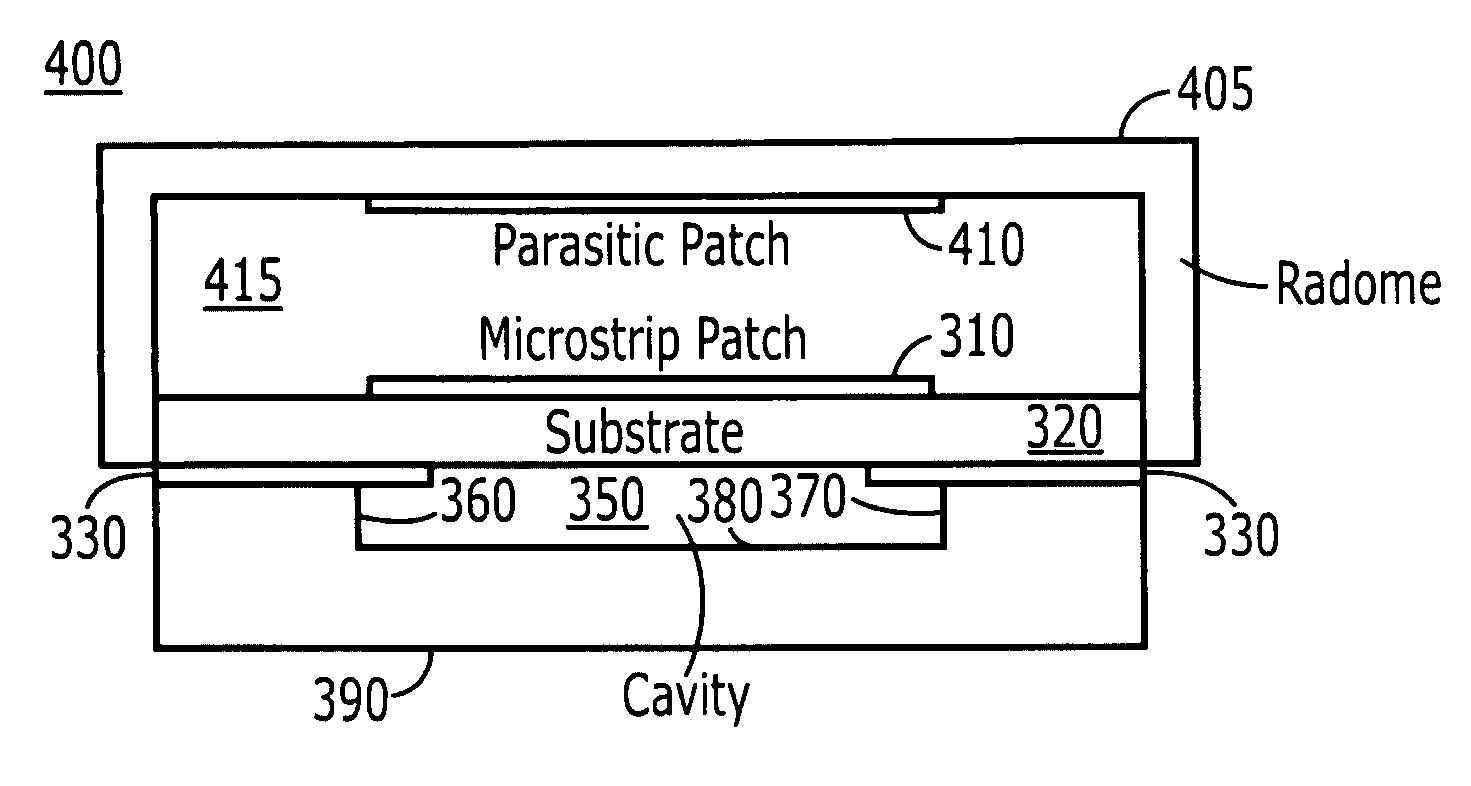
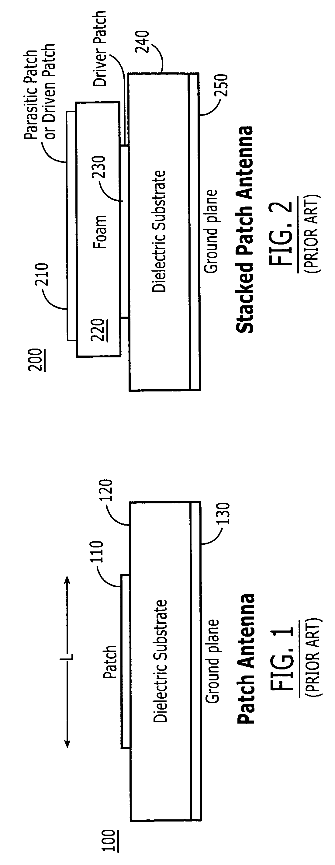
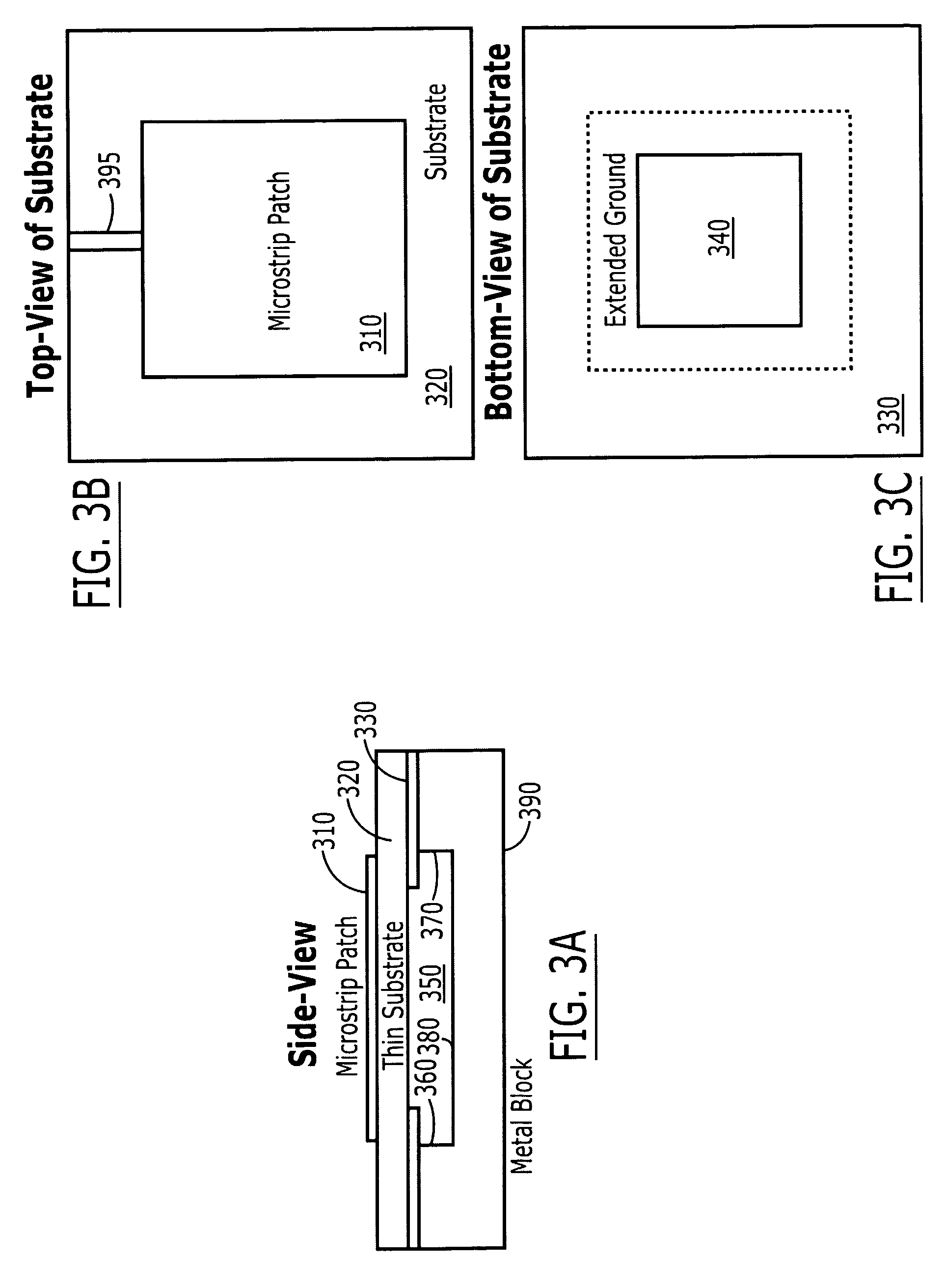
[0023]Referring to FIGS. 3A, 3B, and 3C, an embodiment of the broadband patch antenna 300 is shown in a cross-sectional view (FIG. 3A), a top view (FIG. 3B) and a bottom view (FIG. 3C). The illustrated device comprises a base layer 390 having a cavity 350, a ground plane 330 having an opening 340 (shown in FIG. 3C), a dielectric substrate 320, and a driver patch 310. As in conventional patch antenna 100 described above, an input signal is preferably provided to the driver patch 310 via a microstrip line 395 (in FIG. 3B) and radiated outward by driver patch 310. Alternatively, the input signal may be provided via a coaxial probe feed passing upward through the base layer 390, cavity 350, and opening 340 to the driver patch 310.

[0024]The opening of the ground plane 330 may be larger than, coextensive with, or smaller than the cavity or the driver patch 310. Ground plane 330 is preferably extended beneath driver patch 310, such that at least a portion of the ground plane 330 overlaps t...


PUM


Abstract

The invention provides a compact patch antenna having a cavity underneath the driver patch, so that the electromagnetic volume of the antenna is expanded without increasing the overall area of the antenna. More specifically, the compact patch antenna comprises a base layer having a cavity, a ground plane located on the base layer, and having an opening over at least a portion of the cavity, a substrate located on the ground plane, and a driver patch located on the substrate. The invention further provides a method for constructing a compact patch antenna, comprising the steps of providing a base layer having a cavity, providing a ground plane located on the base layer, and having an opening over at least a portion of the cavity, providing a substrate located on the ground plane, and providing a driver patch located on the substrate.

Description

FIELD OF THE INVENTION[0001]The present invention relates to communications antennas, and more specifically relates to a novel microstrip patch antenna suitable for use in an antenna array.BACKGROUND OF THE INVENTION[0002]A modern trend in the design of antennas for wireless devices is to combine two or more antenna elements into an antenna array. Each antenna element in such an array should have a small footprint, a low level of mutual coupling with neighboring elements, a low element return loss, a low axial ratio (in case of circular polarization), and a large frequency bandwidth. For a typical antenna element in an antenna array, however, these requirements are typically at odds with each other. For example, the larger the bandwidth and the larger the size of an antenna element, the stronger will be the mutual coupling between the antenna element and its neighboring elements in the antenna array.[0003]FIG. 1 depicts a conventional patch antenna element 100 for use in an antenna ...

Claims


Application Information

Patent Timeline
Patent Type & Authority Patents(United States)
IPC IPC(8): H01Q1/38
CPCH01Q9/0442H01Q9/0407
Inventor CHANNABASAPPA, ESWARAPPA
Owner CAES SYST LLC
Why Eureka
Try Eureka