Semiconductor device, display module, and manufacturing method of semiconductor device

a semiconductor and display module technology, applied in the field of semiconductor devices, can solve the problems of large cost to the manufacturing cost of liquid crystal modules, poor adhesion strength between the insulating film substrate b>101/b> and the anisotropic conductive adhesive, and foregoing conventional problems, etc., to achieve the effect of improving adhesion

Active Publication Date: 2009-12-29
SHENZHEN TOREY MICROELECTRONIC TECH CO LTD
View PDF22 Cites 31 Cited by
  • Summary
  • Abstract
  • Description
  • Claims
  • Application Information

AI Technical Summary

Benefits of technology

[0009]An object of the present invention is to provide a semiconductor device, a display module, and a manufacturing method of a semiconductor device, which provide improved adhesion between an insulating film substrate and an anisotropic conductive adhesive, and which require no additional adhesion reinforcing member.
[0011]According to the invention, the surface of the organic insulating film is treated with the silicon coupling material. Thus, in making electrical contacts between the wiring patterns of the semiconductor device and the wirings of external circuit boards with the use of an anisotropic conductive adhesive, the adhesion between the insulating film substrate and the anisotropic conductive adhesive can be improved. There accordingly will be no electrical failure caused by detachment, and application of additional reinforcing materials will not be necessary. As a result, cost is reduced.
[0013]This effectively improves the adhesion between the insulating film substrate and the anisotropic conductive adhesive. There accordingly will be no electrical failure caused by detachment, and application of additional reinforcing materials will not be necessary. As a result, cost is reduced.
[0014]Thus, with the semiconductor device, the adhesion between the insulating film substrate and the anisotropic conductive adhesive can be improved, and no additional adhesion reinforcing member will be required.
[0016]Thus, with the display module, the adhesion between the insulating film substrate and the anisotropic conductive adhesive can be improved, and no additional adhesion reinforcing member will be required.
[0018]Thus, with the manufacturing method of a semiconductor device, the adhesion between the insulating film substrate and the anisotropic conductive adhesive can be improved, and no additional adhesion reinforcing member will be required.

Problems solved by technology

A problem of such a conventional semiconductor device and its display module and manufacturing method, however, is the poor adhesion strength between the insulating film substrate 101 and the anisotropic conductive adhesive 111.
This adds a large cost to the manufacturing cost of the liquid crystal module.
However, even with such a semiconductor device and its display module and manufacturing method, the foregoing conventional problem remains because it still requires the additional reinforcing material 112 and 113.

Method used


Image

  • Semiconductor device, display module, and manufacturing method of semiconductor device
  • Semiconductor device, display module, and manufacturing method of semiconductor device
  • Semiconductor device, display module, and manufacturing method of semiconductor device

Examples


example 1

[0076]In order to confirm effects of the foregoing structure, evaluation experiments were conducted in the manner described below.

[0077]First, evaluation was made as to the adhesion strength between the insulating film surface-treated with the silicon coupling material 31, and the anisotropic conductive adhesive 11.

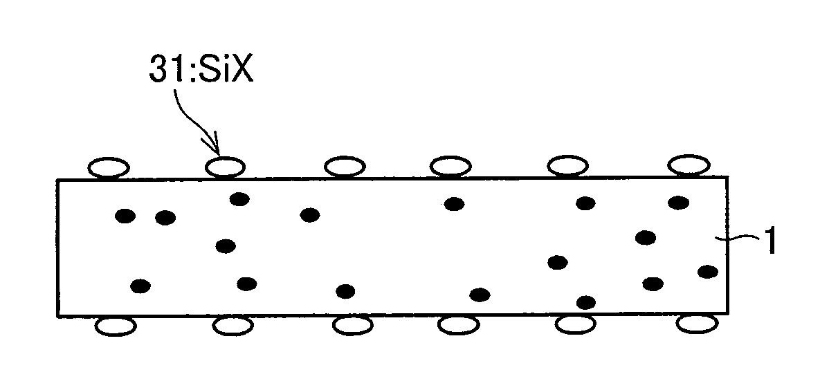
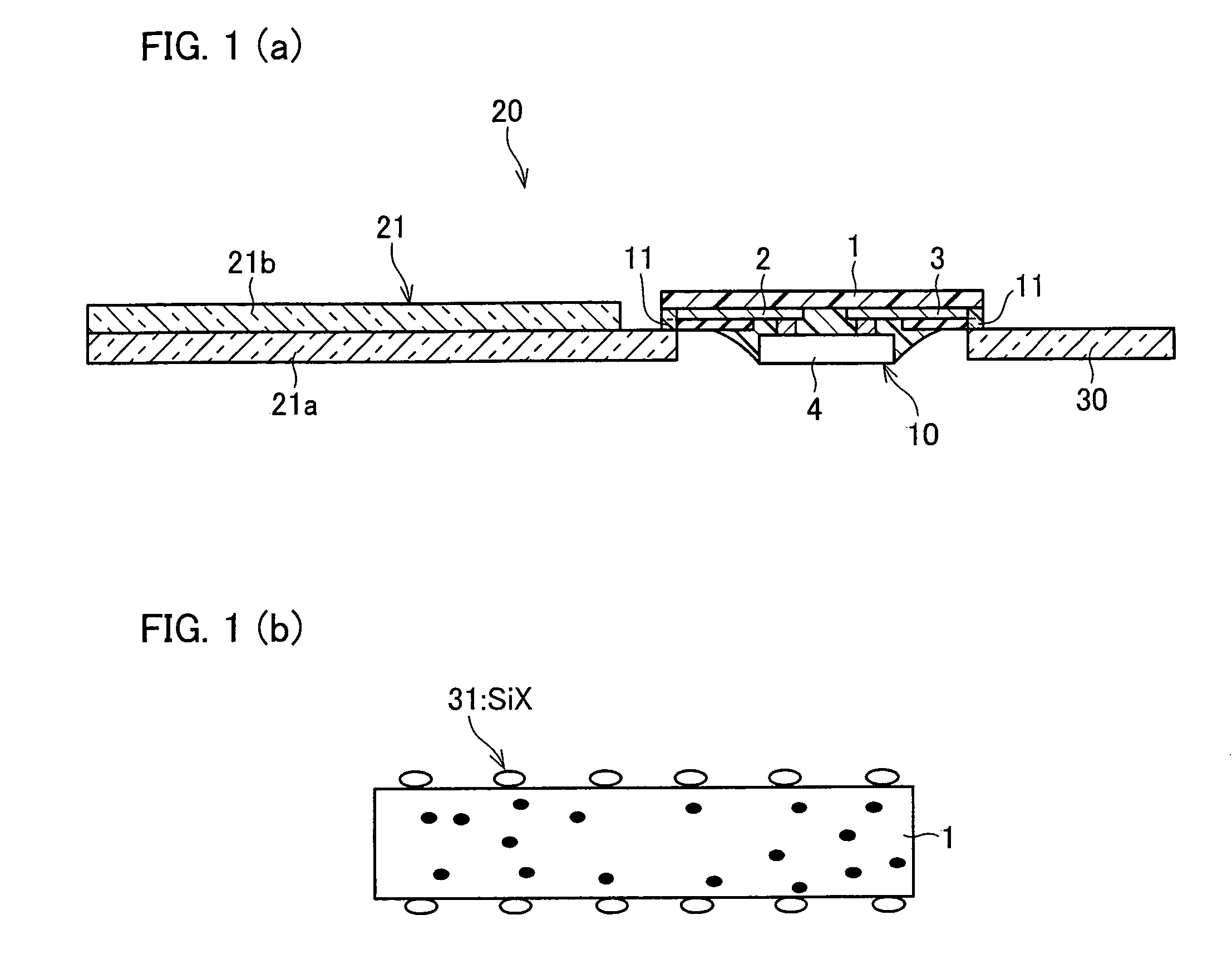
[0078]The silicon coupling material 31 contained SiX in a solvent. The surface of the insulating film had SiX in a range of 0.5 atomic percent to 12.0 atomic percent (surface element density).

[0079]The adhesion strength was measured according to the following procedure. First, as shown in FIG. 5, the TFT substrate 21a of the liquid crystal display panel 21 was bonded to the insulating film forming the substrate 1, with the anisotropic conductive adhesive 11 in between. Then, the insulating film was pulled with a pulling jig at a pulling angle of 90°.

[0080]As a result, as shown in FIG. 6(b), there was improvement of adhesion strength 0 hour, 100 hours, 300 hours, and 500 h...

example 2

[0082]Manufacture of the liquid crystal module 20 involves washing with a solvent. As such, solvent resistance to solvents was also examined by experiment.

[0083]As the solvents, isopropyl alcohol and acetone were used that are commonly used for washing. In the experiment, an insulating film surface-treated with the silicon coupling material 31 was immersed in isopropyl alcohol and acetone for one hour at ordinary temperature, and the film was observed by visual inspection. As in the foregoing experiment, the surface element density of the silicon coupling material 31 on the surface of the insulating film was 0.5 atomic percent to 12.0 atomic percent.

[0084]As summarized in Table 1 below, insulating films surface-treated with the silicon coupling material 31 had no detaching, swelling, dissolving, or cracking, as with insulating films with no surface treatment.

[0085]

TABLE 1COF W / O SURFACECOF WITH SURFACESOLVENTSAMPLETREATMENTTREATMENTISOPROPYL1NO DETACHING,NO DETACHING,ALCOHOLSWELLING...


PUM

PropertyMeasurementUnit
particle diameteraaaaaaaaaa
thickaaaaaaaaaa
pulling angleaaaaaaaaaa

Abstract

A semiconductor device is provided that includes wiring patterns on a substrate formed of an organic insulating film, and a semiconductor chip mounted on the substrate. A liquid crystal display panel and a PW board are electrically connected to each other with an anisotropic conductive adhesive. At least one surface of the insulating film is treated with a silicon coupling material. The silicon coupling material contains silicon (Si) at a surface element density of 0.5 atomic percent to 12.0 atomic percent on a surface of the insulating film.

Description

[0001]This Nonprovisional application claims priority under 35 U.S.C. § 119(a) on Patent Application No. 010847 / 2005 filed in Japan on Jan. 18, 2005, the entire contents of which are hereby incorporated by reference.FIELD OF THE INVENTION[0002]The present invention relates to a semiconductor device, called COF (Chip On FPC, Chip On Film), in which wiring patterns are formed on a substrate formed of an organic insulating film, and in which a semiconductor chip is connected to the wiring patterns. The invention also relates to a display module, and a manufacturing method of such a semiconductor device.[0003]Examples of a display module include: a liquid crystal display module of, for example, an active-matrix type; an electrophoretic display, twist-ball display, a reflective display using a micro prism film, a digital mirror display, and similar types of displays employing a light modulation device; an organic EL light emitting element, inorganic EL light emitting element, a LED (Ligh...

Claims


Application Information

Patent Timeline
Patent Type & Authority Patents(United States)
IPC IPC(8): H01L23/34H01L23/52H01L23/04H01L23/40H01L23/48
CPCH01L23/4985H05K3/323H05K3/389G02F1/13452H01L2924/07811H01L2924/19105H01L2224/73204H01L2224/32225H01L2224/16225H01L2924/12044H05K1/0393H05K1/189H05K2201/0239H01L2924/00H01L2924/00014H01L2924/00011H01L2224/0401A45F5/00F21V33/0004A45F2005/006A45F2200/0516
Inventor TANAKA, YASUHIKOTOYOSAWA, KENJI
Owner SHENZHEN TOREY MICROELECTRONIC TECH CO LTD
Why Eureka
Try Eureka