Substrate with via and pad structures

a technology of via and pad, applied in the field of substrate with via and pad structure, can solve the problems of degrading performance at high frequencies, increasing trace inductance, etc., and achieves the effects of reducing solder formation, increasing solder formation, and high component density

Active Publication Date: 2010-01-12
BRIGHT MASCH INC +1
View PDF17 Cites 32 Cited by
  • Summary
  • Abstract
  • Description
  • Claims
  • Application Information

AI Technical Summary

Benefits of technology

[0005]The present invention relates to a substrate with via and pad structures for use in circuit assemblies. In an embodiment, the substrate has one or more via and pad structures for connecting a component to conductive layers associated with the substrate. The via and pad structure includes a plated via connected to associated conductive layers, a solder mask surrounding the plated via, and a conductive pad with a conductive trace connected to the plated via, wherein the conductive pad extends beyond the terminal sides of the component to increase solder formation at the terminal sides and the solder mask reduces solder formation at the terminal end of the component. The via and pad structures are applicable to the circuit layouts for a variety of components and high component density can be achieved with reliable solder joints to the component terminal sides rather than the terminal end. The invention also provides a method for calculating the distance the conductive pad extends beyond the terminal side of a component.

Problems solved by technology

Another approach to reduce solder wicking is to move the conductive pad 18 further from the via hole 8, but this requires a long conductive trace, such as that covered by solder mask 17, which increases trace inductance and degrades performance at high frequencies.

Method used


Image

  • Substrate with via and pad structures
  • Substrate with via and pad structures
  • Substrate with via and pad structures

Examples


Embodiment Construction

[0013]The following description includes the best mode of carrying out the invention. The detailed description is made for the purpose of illustrating the general principles of the invention and should not be taken in a limiting sense. The scope of the invention is determined by reference to the claims.

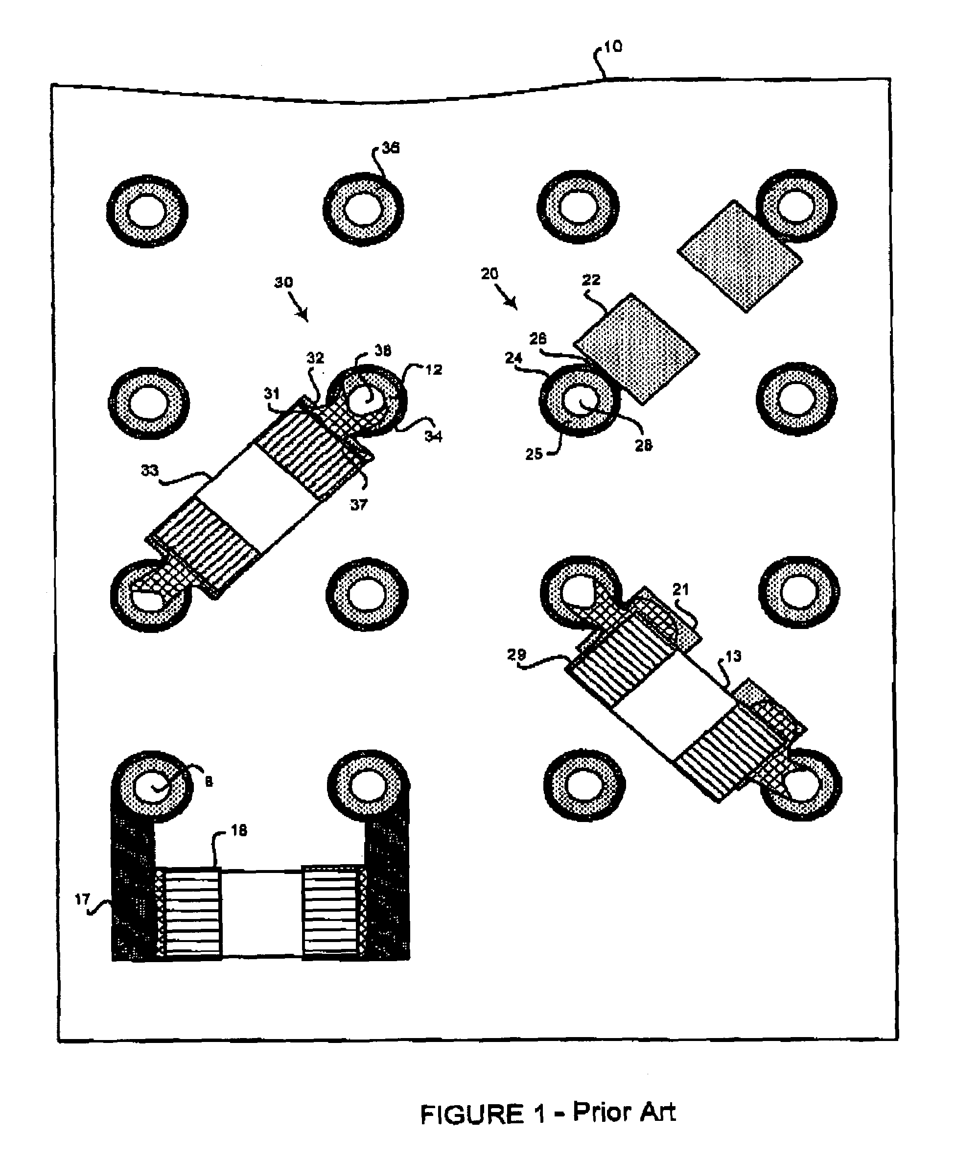
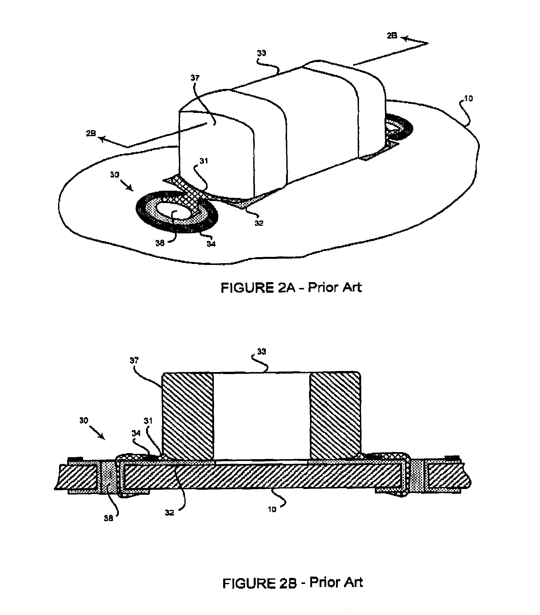
[0014]We assign each part, even if structurally identical to another part, a unique reference number wherever that part is shown in the drawing figures. A dashed circle indicates part of a figure that is enlarged in another figure. Any figure showing the enlarged part is indicated by a reference number tied to the dashed circle.

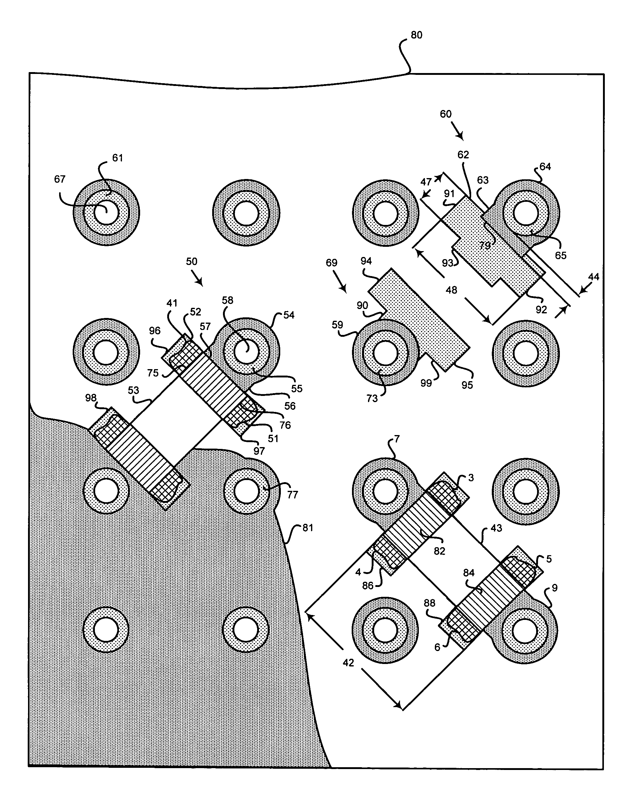
[0015]FIG. 3 illustrates a substrate such as a PWB or a printed circuit board with via and pad structures for connecting surface mount components. A surface mount component such as component 43 has plated terminals 82 and 84 to form solder joints 3, 4, 5, and 6 with corresponding conductive pads 86 and 88. The substrate 80 may include conductive top, bottom, an...


PUM

PropertyMeasurementUnit
widthaaaaaaaaaa
conductiveaaaaaaaaaa
volumeaaaaaaaaaa

Abstract

This invention relates to a substrate with via and pad structure(s) to reduce solder wicking. Each via and pad structure connects a component to conductive layers associated with the substrate. The substrate includes one or more plated vias, solder mask(s) surrounding the plated vias, and a conductive pad with a conductive trace connected to each plated via. The conductive pad extends beyond the terminal sides to increase solder formation and the solder mask reduces solder formation at the terminal end of the component. The via and pad structure is suitable for a variety of components and high component density. The invention also provides a computer implemented method for calculating the maximum distance of a conductive pad extending beyond the terminal side of a component.

Description

BACKGROUND[0001]The present invention relates to a substrate with one or more via and pad structures for use in circuit assemblies with high reliability and high yield in manufacturing.[0002]FIG. 1 illustrates a printed wiring board (PWB) with a substrate 10 having several plated vias such as plated via 35. Each plated via connects to associated conductive layers of the substrate 10. The conductive layers are located on the top, bottom, and / or in the substrate 10. Another structure is the via and pad structure such as via and pad structure 20 shown without a component. Via and pad structure 20 includes a solder mask 24, and a conductive trace 26 connecting a conductive pad 22 and a plated via 25 with a via hole 28.[0003]FIG. 1 also illustrates that when conductive pad 32 is close to the via hole 38 the solder mask 34 will not prevent the solder from being siphoned into the via hole 38. The small amount of solder remaining will form an unreliable solder joint 31 at the terminal end 3...

Claims


Application Information

Patent Timeline
Patent Type & Authority Patents(United States)
IPC IPC(8): H05K1/00H05K1/11H05K3/34
CPCH05K1/114H05K3/3442H05K1/115H05K3/3452H05K2201/09381Y10T29/49165H05K2201/10636Y10T29/49144H05K2201/099Y02P70/50
Inventor SHEPHERD, GLEN C.BURTON, ANTHONY AARON LYNNNG, MICHAEL RYANTANTILLO, MIMI MUNSONTRAN, DIEU-HUONG NGUYEN
Owner BRIGHT MASCH INC
Why Eureka
Try Eureka