Under-bump metallization layers and electroplated solder bumping technology for flip-chip

a technology of electroplated solder and metallization layer, which is applied in the direction of semiconductor devices, semiconductor/solid-state device details, electrical apparatus, etc., can solve the problems of low photoresist performance, imc layer degrades the reliability of solder bumps, and imc layer thickens during device long-time storage, etc., to achieve the effect of improving the photoresist process

Active Publication Date: 2005-01-20
THE HONG KONG UNIV OF SCI & TECH
View PDF13 Cites 61 Cited by
  • Summary
  • Abstract
  • Description
  • Claims
  • Application Information

AI Technical Summary

Benefits of technology

[0014] In accordance with the present invention, an improved method of forming solder bumps for flip chip are described and illustrated. The present invention introduces a thin film including its characteristics, design, and manufacturing method. The thin film is called as Bump-Reflow-Control (BRC) Layer in the present invention. The material characteristics of BRC layer is any kind of thin film material that the solder cannot adhere and bond to the surface of BRC layer during the reflowing process. The present patent also provides a method of design and manufacturing for an improved structure of the UBM layer that consists of the BRC layer and a few metal layers with designed patterns. The improved UBM layer including the BRC layer can improve the formation of solder bumps.
[0016] According to the present invention, a method of forming low-cost and simpler thick photoresist is described and illustrated including a series of photolithography processes, a relevant part design and manufacturing, and a few relevant mask designs.
[0017] In accordance with the last embodiment of the present invention, a mechanical part 7 designed with a hermetic cover is described and illustrated as shown in FIG. 2. It is used to improve the photoresist process. The function of part designed should eliminate the relative air flow between the space 8 air and the wafer 1. During the spin coating photoresist, the wafer is put into the part. A vacuum system path is fabricated in the substrate 17 in FIG. 2. The wafer will be held by the vacuum system when the part 7 spins at a high speed. The spinning speed will increase step by step. The distance between the wafer and the cover is from 3 mm to 10 mm. The hermetical structure can keep the solvent in the photoresist from the evaporation.

Problems solved by technology

Due to the requirements of expensive equipments and complicated process control, the technique isn't used widely.
But the growth of thick IMC layer will degrade the reliability of solder bump 4 because the IMC layer is a brittle material and it can consume the UBM layer 16.
Furthermore, the IMC layer thickens during device long-time storage and device operations even at room temperature.
Under some loading conditions, cracks initiate and propagate easily at the interface of the solder and IMC layers resulting in mechanical failure of the joints.
Low photoresist thickness during the electroplating process can cause bridging.
The typical photolithography cannot achieve enough thick photoresist film to avoid the bridging between both of solders.
And the pattern holes with straight vertical wall are provided by the costly and complex photoresist process.

Method used


Image

  • Under-bump metallization layers and electroplated solder bumping technology for flip-chip
  • Under-bump metallization layers and electroplated solder bumping technology for flip-chip
  • Under-bump metallization layers and electroplated solder bumping technology for flip-chip

Examples


Embodiment Construction

[0025] According to the present invention, an application demonstration is described using some relevant materials. The detailed processes, method and designs are illustrated according to the drawings.

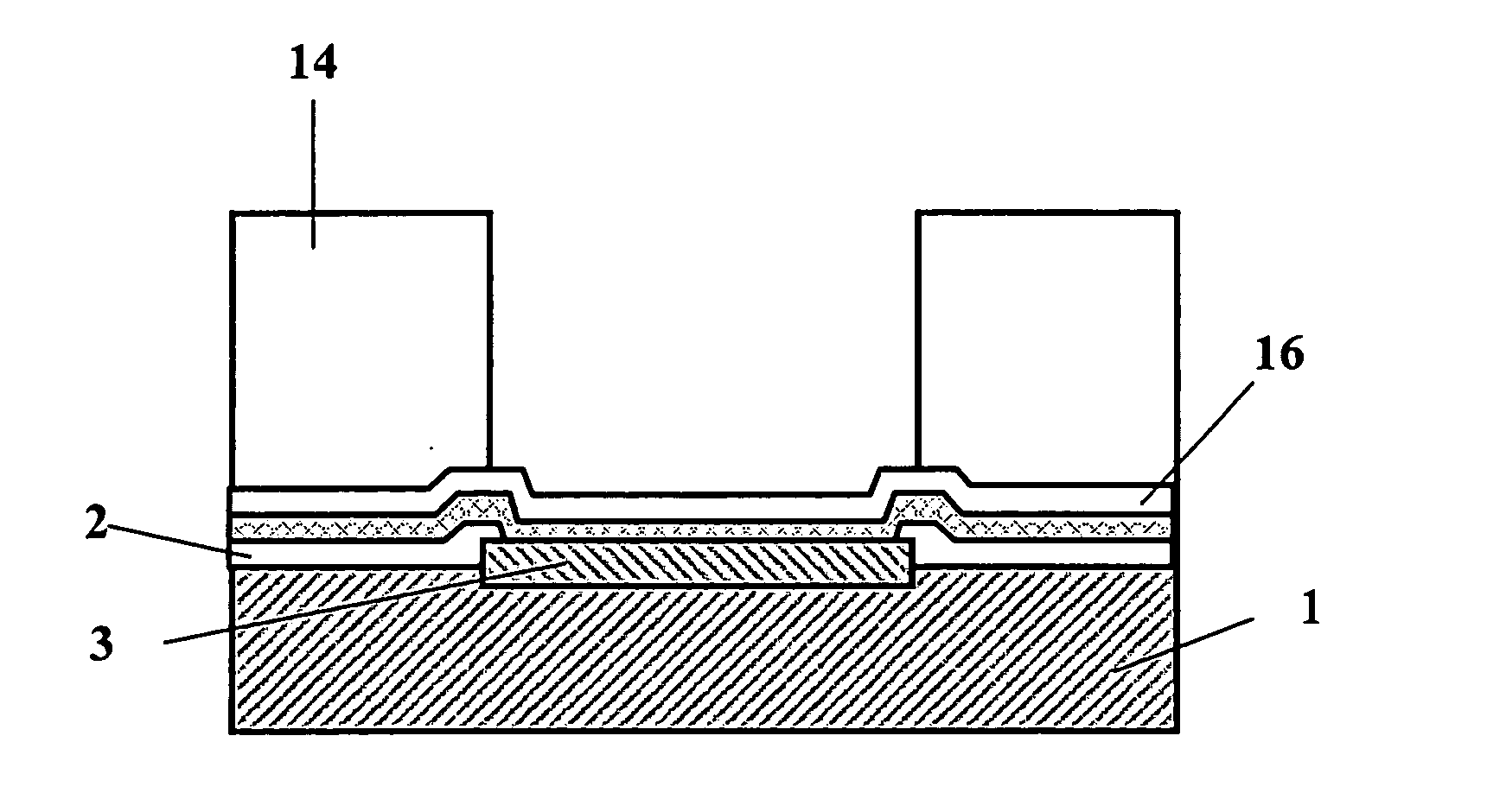
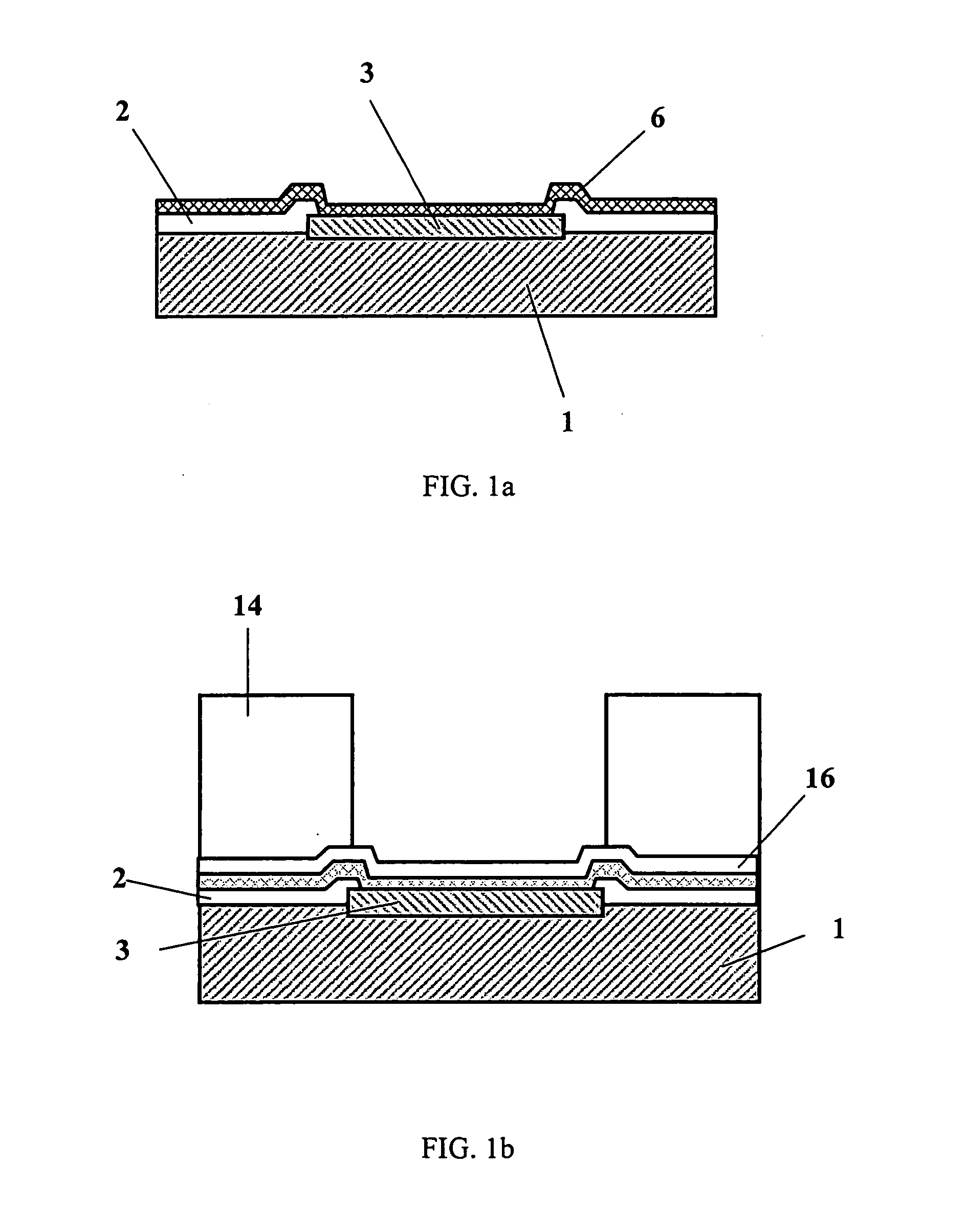
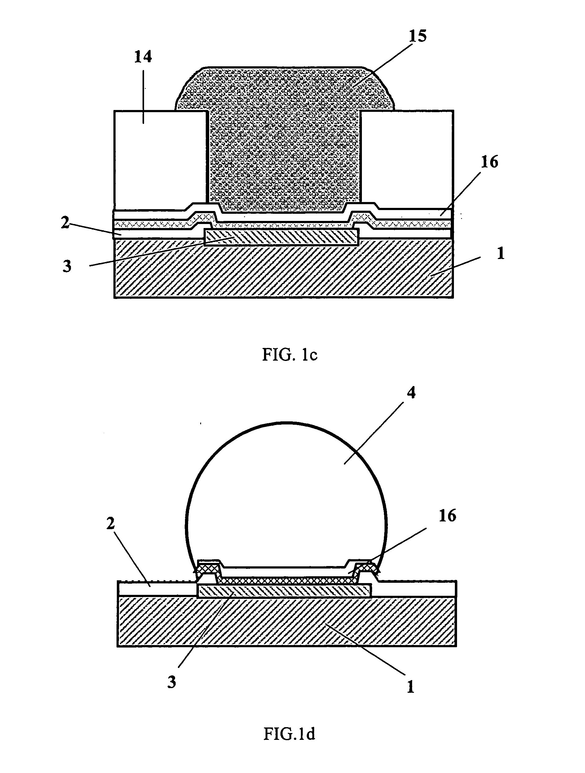
[0026]FIGS. 3a-3c illustrate a method of forming the improved UBM structures and BRC layer. FIG. 3a shows the interconnection metal 3 and the passivation layer 2 have deposited on the wafer 1. A Ti—W alloy layer 18 is deposited by the sputtering process on the wafer 1 firstly. The thickness of Ti—W alloy is between 50 nm and 120 nm. A Cu layer 19 is then deposited on the layer 18. The thickness of layer 19 is between 200 nm and 600 nm. Both of layers are prepared in vacuum system at the same time. And then the organic BRC layer is prepared using a photo-sensitive polyimide. The polyimide layer 9 is coated by the spinning process on the wafer, as shown in FIG. 3b. A thickness of formed thin film 9 is less than 150 nm. The polyimide layer 9 is exposed and patterned by the photolithograp...


PUM

PropertyMeasurementUnit
thicknessaaaaaaaaaa
thicknessaaaaaaaaaa
thicknessaaaaaaaaaa

Abstract

A series of improved processes and methods to manufacture solder bumps on the wafer which shrink the space among solder bumps and reduce the cost of manufacturing. A design method and a relevant manufacturing process are introduced to form an organic material or metal material layer, which is called a Bump-Reflow-Control Layer. The pad patterns can be defined by this method. A mechanical part is designed with a hermetic cover to improve the photoresist process. The series of photolithography process including the designing method of related photolithography mask is introduced to achieve the high quality and thick photoresist.

Description

CROSS-REFERENCE TO RELATED APPLICATIONS [0001] The present application claims priority of CN 03140656.4, which was filed in China on May 31, 2003, the entire contents of which is incorporated herein by reference. FIELD OF THE INVENTION [0002] The present invention relates to electronic packaging, microelectronics fabrication, and more particularly to solder bumps and under bump metallization pads on a wafer or a chip for flip chip attachment. BACKGROUND OF THE INVENTION [0003] Flip chip is an advanced semiconductor interconnection technology. It is also called as Controlled Collapse Chip Connection (C4) that a chip or die is flipped face down and bonded to the substrate with various interconnection materials. The technology is applicable to either single-chip packages or multiple-chip modules. In flip chip attachment, solder bumps deposited on a chip or die are used for electrical interconnection between a chip or an integrated circuit and a substrate. The substrate can be a silicon...

Claims


Application Information

Patent Timeline
Patent Type & Authority Applications(United States)
IPC IPC(8): C25D7/12H01L21/44H01L21/60H01L23/02H01L23/485
CPCH01L24/03H01L2224/119H01L2224/03912H01L2224/0401H01L2224/05147H01L2224/1147H01L2224/11901H01L2224/131H01L2224/29111H01L2924/01005H01L2924/01006H01L2924/01013H01L2924/01014H01L2924/01022H01L2924/01025H01L2924/01028H01L2924/01029H01L2924/01033H01L2924/01046H01L2924/01047H01L2924/0105H01L2924/01074H01L2924/01078H01L2924/01079H01L2924/01082H01L2924/01327H01L2924/014H01L2924/05042H01L2924/09701H01L2924/14H01L2924/30107H01L2924/3651H01L24/11H01L2224/11849H01L2924/01076H01L2924/01024H01L2924/01023H01L2924/00013H01L2224/13099H01L2224/0347H01L2224/03914
Inventor CHAN, CHINGHO PHILIPXIAO, GUOWEI DAVID
Owner THE HONG KONG UNIV OF SCI & TECH
Why Eureka
Try Eureka