Multilayer chip varistor

a multi-layer chip and varistor technology, applied in the direction of varistor cores, resistor details, semiconductor devices, etc., can solve the problems of hindering the downsizing of the above-mentioned electronic devices, high mounting costs, and large mounting area of multi-layer chip varistors, so as to reduce mounting area, reduce mounting costs, and facilitate mounting

Inactive Publication Date: 2010-01-19
TDK CORPARATION
View PDF7 Cites 8 Cited by
  • Summary
  • Abstract
  • Description
  • Claims
  • Application Information

AI Technical Summary

Benefits of technology

[0008]An object of the present invention is to provide a multilayer chip varistor permitting a reduction of mounting area, a decrease of mounting cost, and easy mounting.
[0029]The present invention successfully provides the multilayer chip varistor capable of achieving a reduction in the mounting area and achieving easy mounting, while reducing the mounting cost.

Problems solved by technology

However, where the plurality of multilayer chip varistors are mounted, the mounting area of the multilayer chip varistors becomes so large as to hinder downsizing of the aforementioned electronic devices.
Since the plurality of multilayer chip varistors need to be mounted, mounting cost becomes high and mounting steps become complicated.

Method used


Image

  • Multilayer chip varistor
  • Multilayer chip varistor
  • Multilayer chip varistor

Examples


first embodiment

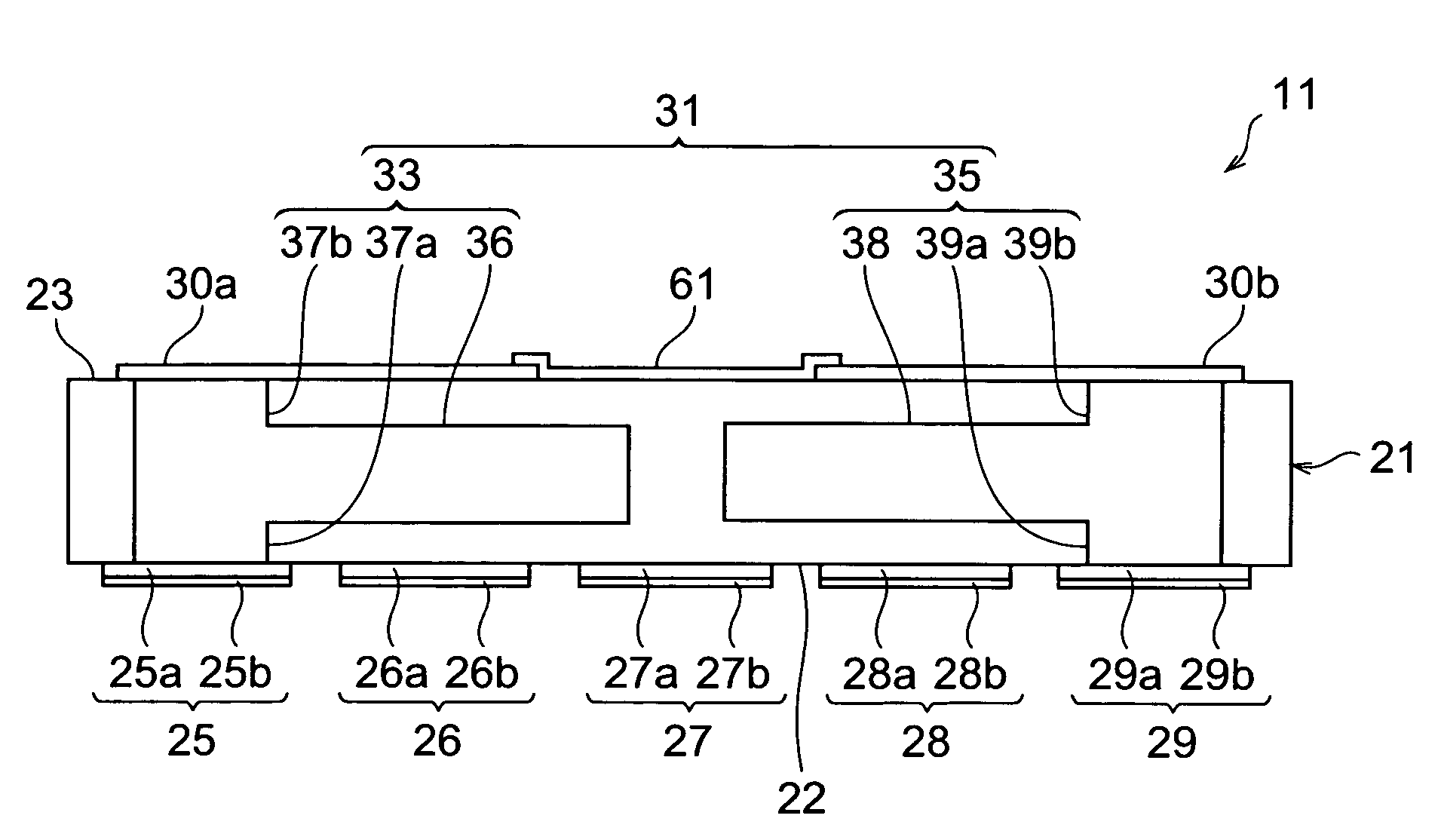
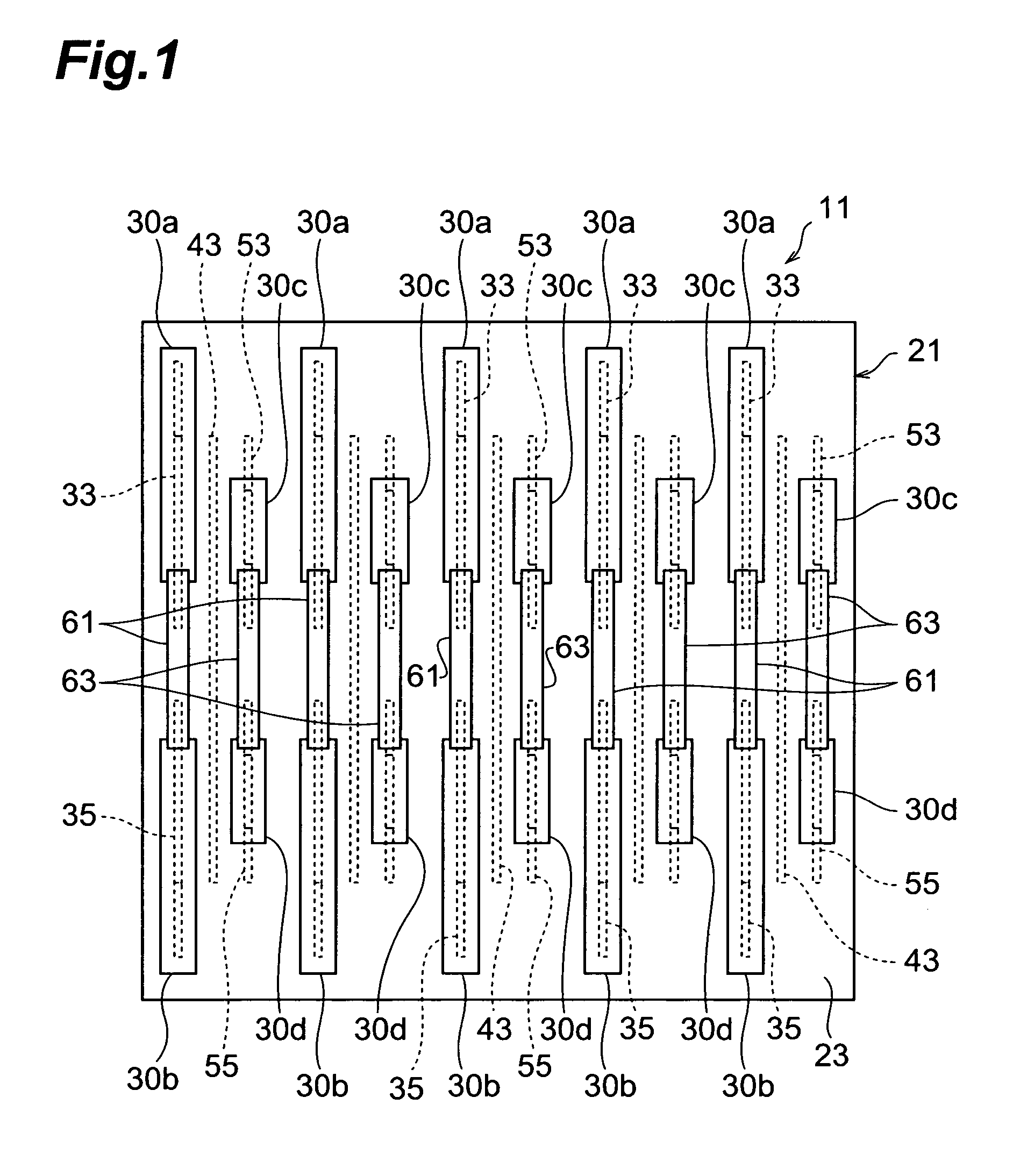
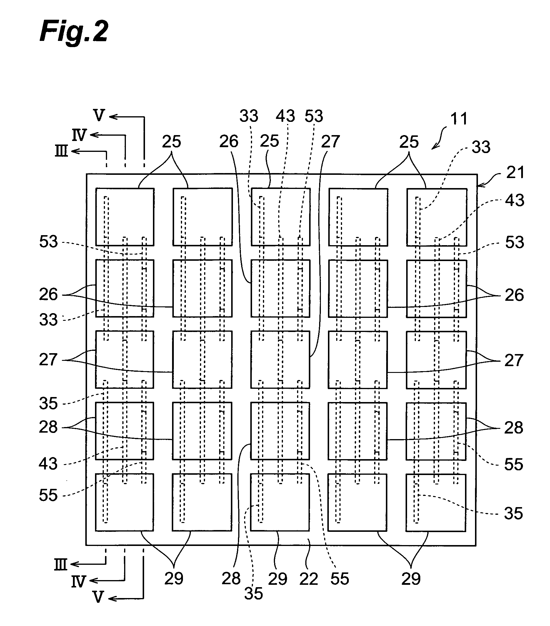
[0051]A configuration of multilayer chip varistor 11 according to the first embodiment will be described with reference to FIGS. 1 to 5. FIG. 1 is a schematic top plan view showing the multilayer chip varistor of the first embodiment. FIG. 2 is a schematic bottom view showing the multilayer chip varistor of the first embodiment. FIG. 3 is a view for explaining a sectional configuration along line III-III in FIG. 2. FIG. 4 is a view for explaining a sectional configuration along line IV-IV in FIG. 2. FIG. 5 is a view for explaining a sectional configuration along line V-V in FIG. 2.

[0052]The multilayer chip varistor 11, as shown in FIGS. 1 to 5, comprises a varistor element body 21 of an approximately rectangular plate shape, a plurality of (twenty five in the present embodiment) external electrodes 25-29, and a plurality of (twenty in the present embodiment) external electrodes 30a-30d. The plurality of external electrodes 25-29 are disposed each on a first principal surface (outer ...

second embodiment

[0096]A configuration of multilayer chip varistor 71 according to the second embodiment will be described with reference to FIGS. 9 to 12. FIG. 9 is a schematic top view showing the multilayer chip varistor according to the second embodiment. FIG. 10 is a schematic bottom view showing the multilayer chip varistor according to the second embodiment. FIG. 11 is a view for explaining a sectional configuration along line XI-XI in FIG. 10. FIG. 12 is a view for explaining a sectional configuration along line XII-XII in FIG. 10.

[0097]The multilayer chip varistor 71, as shown in FIGS. 9-12, has a varistor element body 81 of an approximately rectangular plate shape, and a plurality of (sixteen in the present embodiment) external electrodes 85-88. The plurality of external electrodes 85-88 are disposed each on a first principal surface (outer surface) 82 of the varistor element body 81. The varistor element body 81 has a second principal surface (outer surface) 83 facing the first principal ...


PUM


Abstract

A multilayer chip varistor comprises a multilayer body in which a plurality of varistor portions are arranged along a predetermined direction, and a plurality of terminal electrodes. Each varistor portion has a varistor layer to exhibit nonlinear voltage-current characteristics, and a plurality of internal electrodes disposed so as to interpose the varistor layer between them. Each terminal electrode is disposed on a first outer surface parallel to the predetermined direction out of outer surfaces of the multilayer body and is electrically connected to a corresponding internal electrode out of the plurality of internal electrodes. Each of the plurality of internal electrodes includes a first electrode portion overlapping with another first electrode portion between adjacent internal electrodes out of the plurality of internal electrodes, and a second electrode portion led from the first electrode portion so as to be exposed in the first outer surface. The plurality of terminal electrodes are electrically connected via the respective second electrode portions to the corresponding internal electrodes.

Description

BACKGROUND OF THE INVENTION[0001]1. Field of the Invention[0002]The present invention relates to a multilayer chip varistor.[0003]2. Related Background Art[0004]One of the known multilayer chip varistors of this type is a varistor comprising: a varistor element body having a varistor layer to exhibit nonlinear voltage-current characteristics, and a pair of internal electrodes disposed so as to interpose the varistor layer between them; and a pair of terminal electrodes which are located at two end portions of the varistor element body and each of which is connected to a corresponding internal electrode out of the internal electrodes.SUMMARY OF THE INVENTION[0005]In recent years, the multilayer chip varistors are used as anti-ESD (Electrostatic Discharge) components, in order to protect ICs and others included in various electric circuits in electronic devices such as DSC (Digital Still Camera), DVC (Digital Video Camera), PDA (Personal Digital Assistant), notebook computers, or cell...

Claims


Application Information

Patent Timeline
Patent Type & Authority Patents(United States)
IPC IPC(8): H01C7/10
CPCH01C1/148H01C7/1006H01C7/112H01C7/18H01L29/93
Inventor MORIAI, KATSUNARIMATSUOKA, DAISAITO, YO
Owner TDK CORPARATION
Why Eureka
Try Eureka