Focus ring and plasma processing apparatus

a technology of plasma processing apparatus and focus ring, which is applied in the direction of coating, chemical vapor deposition coating, electric discharge tube, etc., to achieve good and uniform process and improve the in-surface uniformity of process

Inactive Publication Date: 2010-02-09
TOKYO ELECTRON LTD
View PDF16 Cites 29 Cited by
  • Summary
  • Abstract
  • Description
  • Claims
  • Application Information

AI Technical Summary

Benefits of technology

[0016]The present invention is conceived from the above conventional drawbacks; and it is, therefore, an object of the present invention to provide a focus ring and a plasma processing apparatus capable of performing a good and uniform process in a peripheral portion of a semiconductor wafer as well as in a central portion of the semiconductor wafer, improving in-surface uniformity in a process and reducing occurrences of deposition on a backside surface side of a peripheral portion of the semiconductor wafer compared to a conventional case.
[0048]In accordance with the present invention, a good and uniform process can be performed in a peripheral portion of a semiconductor wafer as well as in a central portion of the semiconductor wafer and the in-surface uniformity of a process can be improved while occurrences of deposition on a backside surface of a peripheral portion of the semiconductor wafer can be reduced compared to a conventional case.

Problems solved by technology

However, using the focus ring 101 may result in a so-called deposition, in which undesirable deposits made of CF-based polymer and the like are adhered to a backside surface of the peripheral portion (edge portion) of the semiconductor wafer W.

Method used


Image

  • Focus ring and plasma processing apparatus
  • Focus ring and plasma processing apparatus
  • Focus ring and plasma processing apparatus

Examples


Embodiment Construction

[0066]Hereinafter, the present invention will be described in detail with reference to the accompanying drawings.

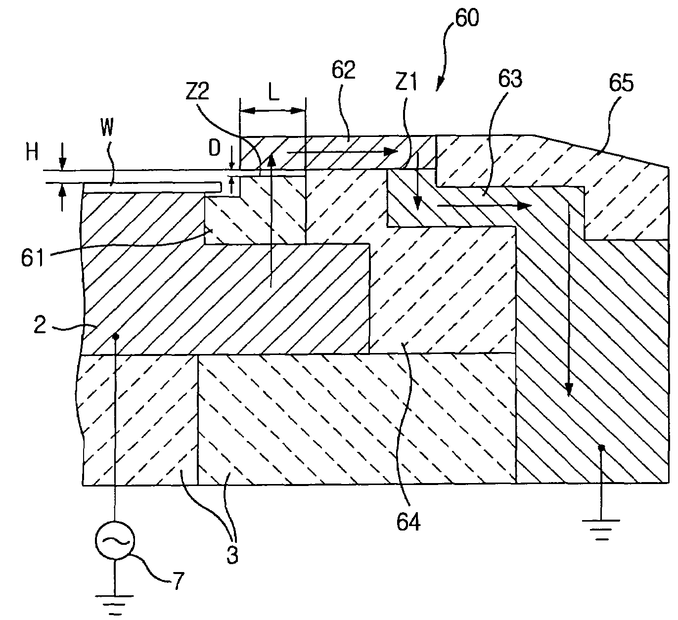
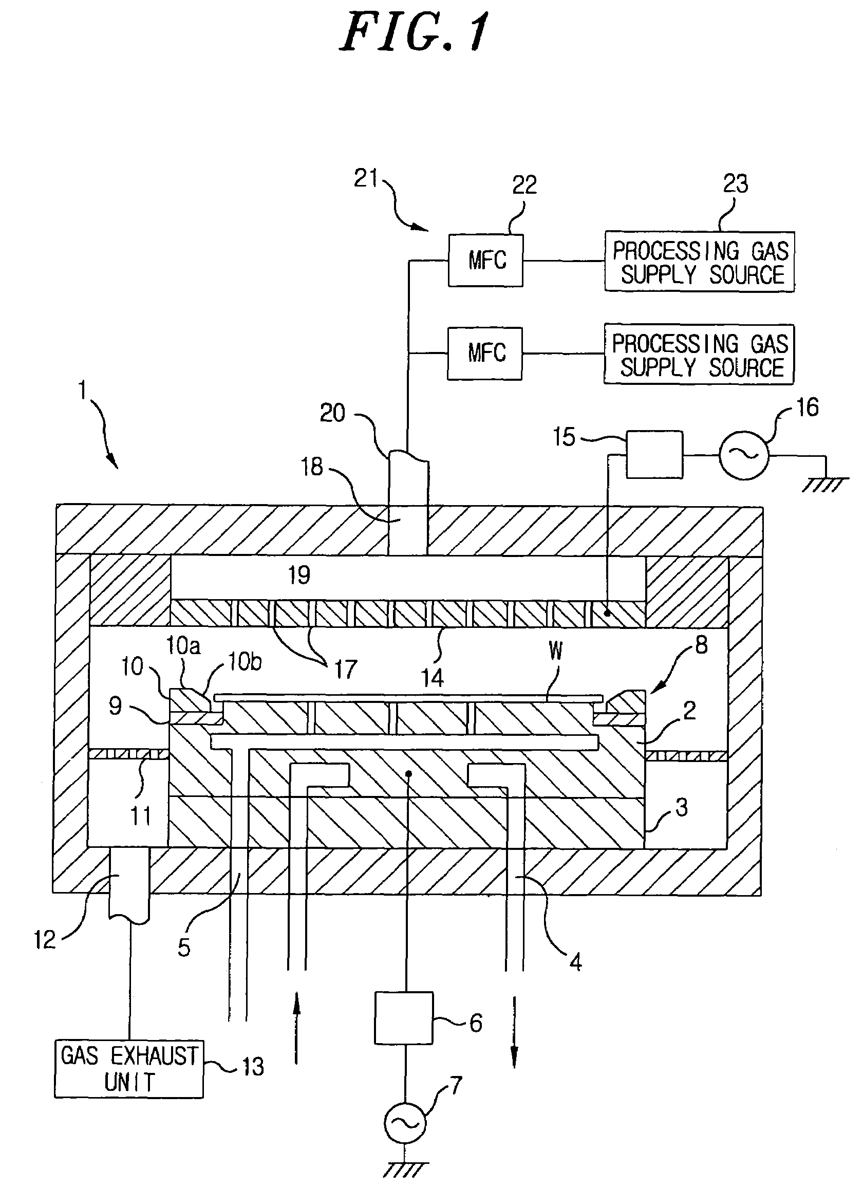
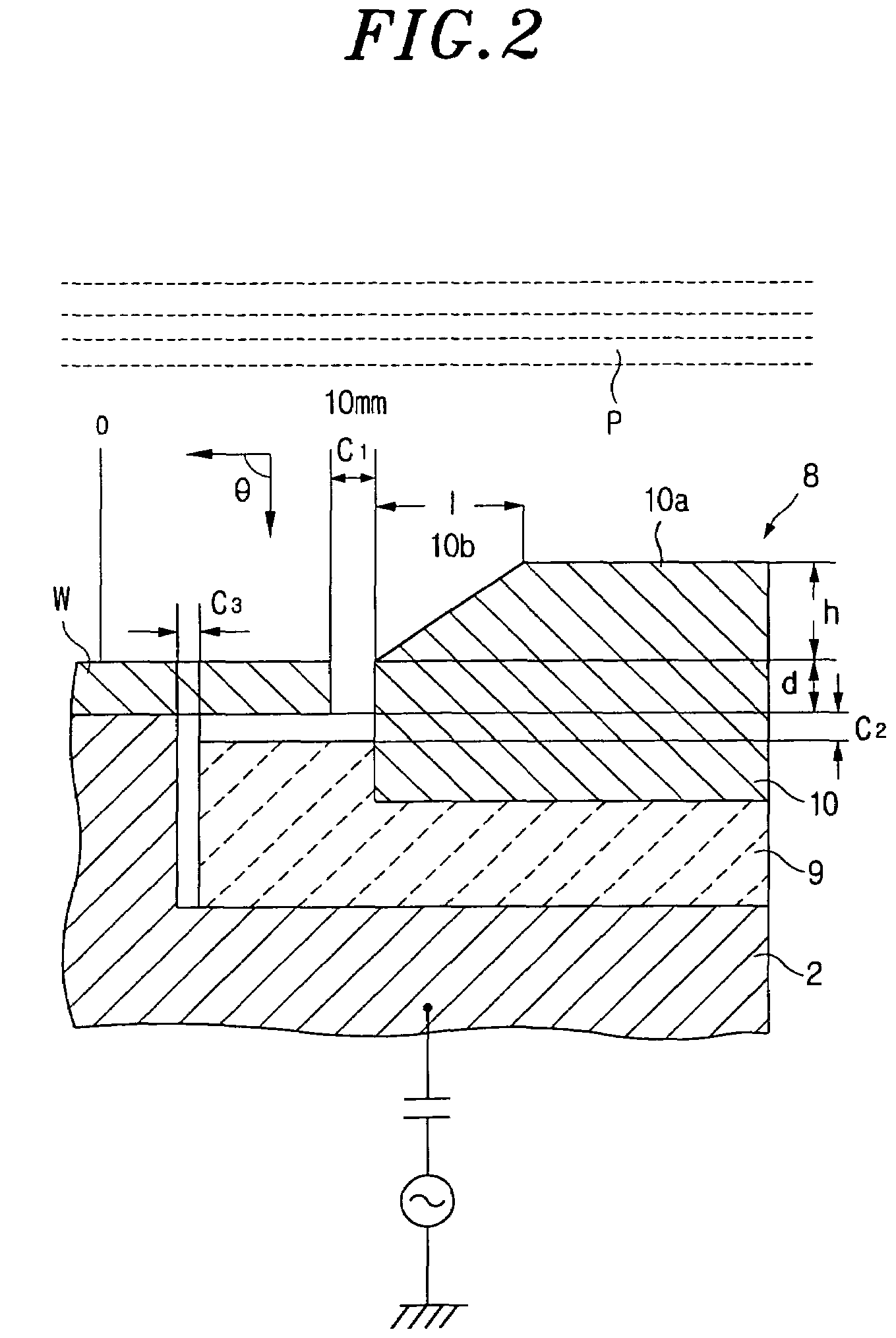
[0067]FIG. 1 shows a schematic configuration of a whole plasma processing apparatus (etching apparatus) in accordance with a preferred embodiment of the present invention. A reference numeral 1 illustrates a cylindrical processing chamber (vacuum chamber) made of aluminum or the like which can be airtightly sealed.

[0068]A susceptor 2 also serving as a lower electrode is installed in the vacuum chamber 1, and the susceptor 2 is formed of a conductive material such as aluminum and has a block shape.

[0069]The susceptor 2 is supported by an insulating plate 3 formed of ceramic or the like in the vacuum chamber 1. An electrostatic chuck (not shown) for attracting and holding the semiconductor wafer W is installed on a semiconductor wafer W mounting surface of the susceptor 2.

[0070]Additionally, installed in the susceptor 2 are a heat transfer medium path 4 for circulating an i...


PUM

PropertyMeasurementUnit
temperatureaaaaaaaaaa
lengthaaaaaaaaaa

Abstract

A focus ring and a plasma processing apparatus capable of improving an in-surface uniformity of a surface and reducing occurrences of deposition on a backside surface of a peripheral portion of a semiconductor wafer compared to a conventional case are provided. Installed in a vacuum chamber is a susceptor for mounting the semiconductor wafer thereon and a focus ring is installed to surround the semiconductor wafer mounted on the susceptor. The focus ring includes an annular lower member made of a dielectric, and an annular upper member made of a conductive material and mounted on the lower member. The upper member includes a flat portion which is an outer peripheral portion having a top surface positioned higher than a surface to be processed of the semiconductor wafer W, and an inclined portion which is an inner peripheral portion inclined inwardly.

Description

FIELD OF THE INVENTION[0001]The present invention relates to a plasma processing apparatus and a focus ring provided in a processing chamber for carrying out a plasma process, e.g., an etching process, on a substrate such as a semiconductor wafer or the like.BACKGROUND OF THE INVENTION[0002]Conventionally, a plasma processing apparatus such as an etching processing apparatus has been widely used in, e.g., a manufacturing process of, e.g., a fine electric circuit of a semiconductor device.[0003]In such a plasma processing apparatus, a substrate to be processed, e.g., a semiconductor wafer, is disposed in a processing chamber whose inner space is configured to be capable of being airtightly sealed, and a plasma is generated in the processing chamber to be applied to the substrate to be processed to be used in performing a plasma process such as an etching.[0004]Further, the plasma processing apparatus may include an annular member called a focus ring disposed to surround a semiconduct...

Claims


Application Information

Patent Timeline
Patent Type & Authority Patents(United States)
IPC IPC(8): C23F1/00C23C16/00H01L21/306
CPCH01J37/32642H01L21/68735H01L21/68757
Inventor KOSHIISHI, AKIRATANAKA, HIDEAKIOKAYAMA, NOBUYUKIMIYAGAWA, MASAAKIMIZUKAMI, SHUNSUKESHIMIZU, WATARUHIROSE, JUNWAKAKI, TOSHIKATSUMIWA, TOMONORIOOYABU, JUNHAYASHI, DAISUKE
Owner TOKYO ELECTRON LTD
Why Eureka
Try Eureka