Integrated passive device and method of fabrication

a passive device and integrated technology, applied in the field of electronic devices, can solve the problems of time delay, cross-talk, and performance of the final semiconductor produ

Inactive Publication Date: 2010-02-16
FREESCALE SEMICON INC
View PDF9 Cites 30 Cited by
  • Summary
  • Abstract
  • Description
  • Claims
  • Application Information

AI Technical Summary

Problems solved by technology

This introduces the problem of increased capacitive coupling between those structures and leads, which produces time delays and creates cross-talk between the wiring elements.
RC (resistance-capacitance resonant) losses in the wiring levels of integrated circuits make significant contributions limiting the performance of the final semiconductor product.
While the use of particular materials or air voids can effectively reduce coupling and RC losses, such structures can increase fabrication complexity, and commensurately, fabrication costs of such integrated circuits.
However, challenges remain in reducing the device footprint relative to the footprint achieved utilizing two-dimensional integration of integrated passive devices and MEMS components, reducing cost, and simplifying fabrication processes.

Method used


Image

  • Integrated passive device and method of fabrication
  • Integrated passive device and method of fabrication
  • Integrated passive device and method of fabrication

Examples


Embodiment Construction

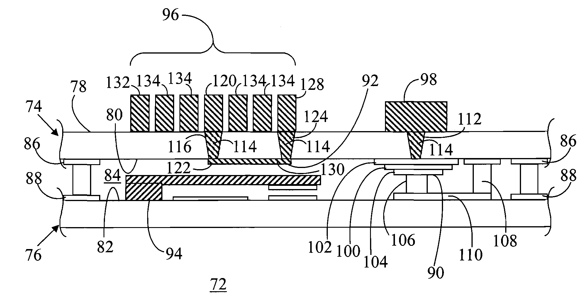
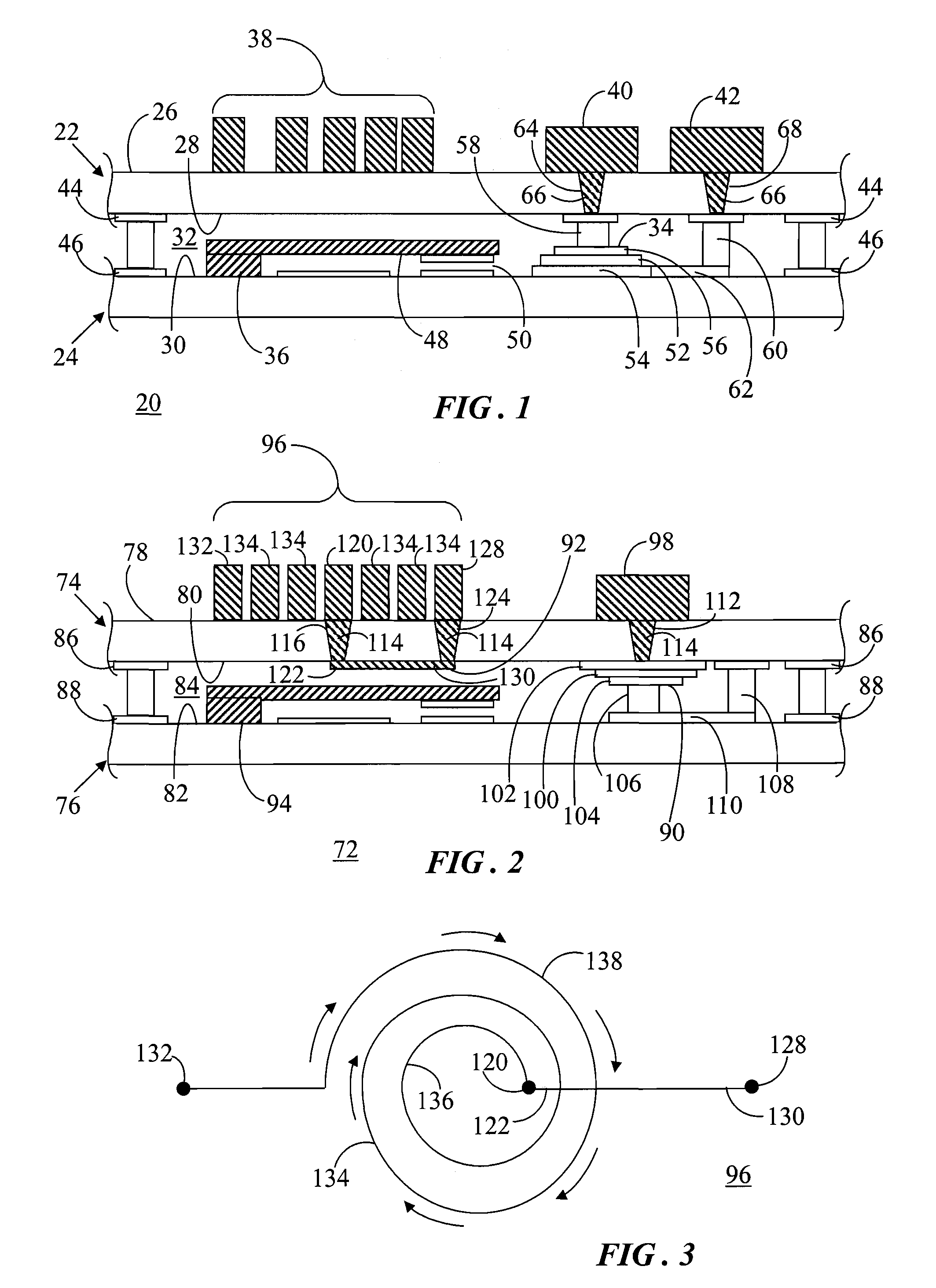
[0014]In one embodiment, an electronic device based upon a three-dimensional integrated passive device architecture includes an integrated passive device, for example, a metal-insulator-metal (MIM) capacitor. The electronic device based upon a three-dimensional integrated passive device architecture may be combined with a micro electro-mechanical systems (MEMS) component in a stacked fashion. The resulting combination can be readily and cost effectively incorporated into existing and upcoming MEMS-based systems. In another embodiment, the electronic device based upon a three-dimensional integrated passive device architecture may further be combined with an underpass transmission line that can be utilized in lieu of a low dielectric material or in lieu of an air bridge to reduce capacitive coupling and RC losses.

[0015]FIG. 1 shows a cross-sectional view of an electronic device 20 in accordance with one embodiment of the present invention. Electronic device 20 includes a substrate 22 ...


PUM


Abstract

A device 20 includes substrates 22 and 24 coupled to form a volume 32 between the substrates. A surface 28 of the substrate 22 faces a surface 30 of the substrate 24. A metal-insulator-metal capacitor 34 is formed on one of the surfaces 28 and 30. A conductive element 58 spans between a top electrode 56 of the capacitor 34 and the other surface 28 and 30. Vias 64 and 66 extend through the substrate 22 and are electrically interconnected with the conductive element 58 and a bottom electrode 52 of the capacitor 34. Another device 72 includes an underpass transmission line 92 formed on a surface 80 of a substrate 74 within a volume 84 formed between the substrate 74 and another substrate 76. The line 92 underlies an integrated device 96 formed on a surface 78 of the substrate 74.

Description

TECHNICAL FIELD OF THE INVENTION[0001]The present invention relates generally to electronic devices. More specifically, the present invention relates to electronic devices fabricated using integrated passive device (IPD) technology.BACKGROUND OF THE INVENTION[0002]The explosion of growth in the portable wireless electronics industry has provided numerous challenges and opportunities for manufacturers of integrated circuits. The latest portable wireless telephony, data, and Internet access products demand greater functionality, higher performance, and lower cost in smaller and lighter formats. Additionally, wireless applications are spreading to new markets—from radar-equipped passenger vehicles to biomedical devices that, when injected or inserted, send data to a receiver outside the body. This demand has been satisfied in part by major advances in integrated circuit (IC) device technology and by the introduction of smaller packaging form factors, smaller discrete passive components...

Claims


Application Information

Patent Timeline
Patent Type & Authority Patents(United States)
IPC IPC(8): H01L27/14H01L29/00H01L29/82H01L29/84
CPCB81C1/00253H01L28/10H01L28/60
Inventor LIU, LIANJUNMILLER, MELVY F.
Owner FREESCALE SEMICON INC
Why Eureka
Try Eureka