Booster circuit

a booster circuit and circuit technology, applied in the direction of dc-dc conversion, power conversion systems, instruments, etc., can solve the problems of increasing the manufacturing cost of the circuit, not enough of the integrated capacitor to satisfy the required capacitance value, and the output voltage drops in a relatively short period of time, so as to suppress the effect of boosting the voltage and suppressing the increase in the number of external capacitors

Active Publication Date: 2010-02-16
RENESAS ELECTRONICS CORP
View PDF44 Cites 23 Cited by
  • Summary
  • Abstract
  • Description
  • Claims
  • Application Information

AI Technical Summary

Benefits of technology

[0010]This makes it possible to suppress an increase in a number of an external capacitor for setting an output voltage of the booster circuit constant.
[0012]The output voltage is set based on the boosted voltage. This boosted voltage is gained by boosting the input voltage M times. This makes it possible to suppress an increase in a number of an external capacitor for setting an output voltage of the booster circuit constant.
[0013]In still another embodiment, a charge pump type booster circuit generates a positive or negative boosted output voltage. The charge pump type booster circuit includes a first booster path connected between an input terminal and an output terminal to output the positive or negative boosted output voltage gained by boosting an input voltage through N (N is a positive integer of two or more) capacitors; and a second booster path connected between the input terminal and the output terminal to output the positive or negative boosted output voltage gained by boosting the input voltage through M (M is a positive integer of less than N) capacitor. This makes it possible to suppress an increase in a number of an external capacitor for setting an output voltage of the booster circuit constant.

Problems solved by technology

However, in a charge pump type booster circuit, the output voltage drops in a relatively short period of time when a value of a current flowing to a load becomes larger.
Because the charge pump type booster circuit requires a large capacitance value, it is often not enough for an integrated capacitor to satisfy the required capacitance value.
In this case, an increase in a number of the capacitors results in an increase of manufacturing cost of the circuit.
When a plurality of booster units as shown in FIG. 9 are used so as to suppress ripples of the output voltage, manufacturing cost of the circuit raises accordingly and it becomes difficult to suppress the cost up of the circuit.
As explained above, it was difficult to suppress a total number of external capacitors so as to keep the output voltage constant.

Method used


Image

  • Booster circuit
  • Booster circuit
  • Booster circuit

Examples


first embodiment

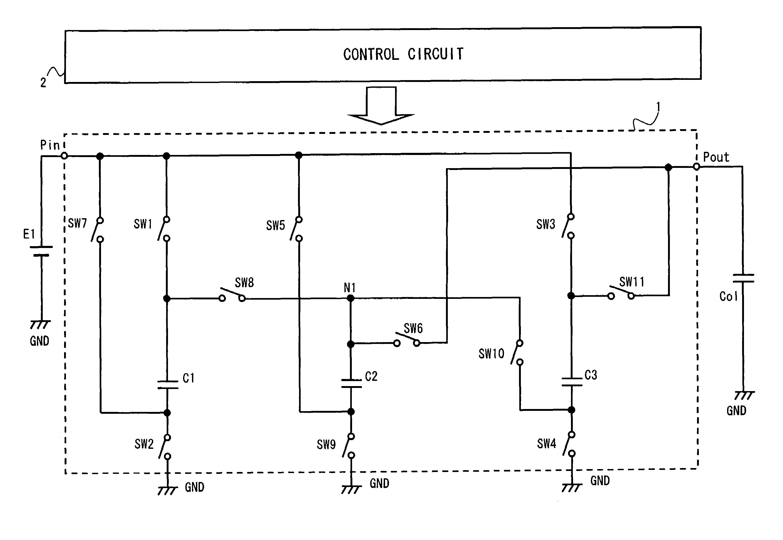
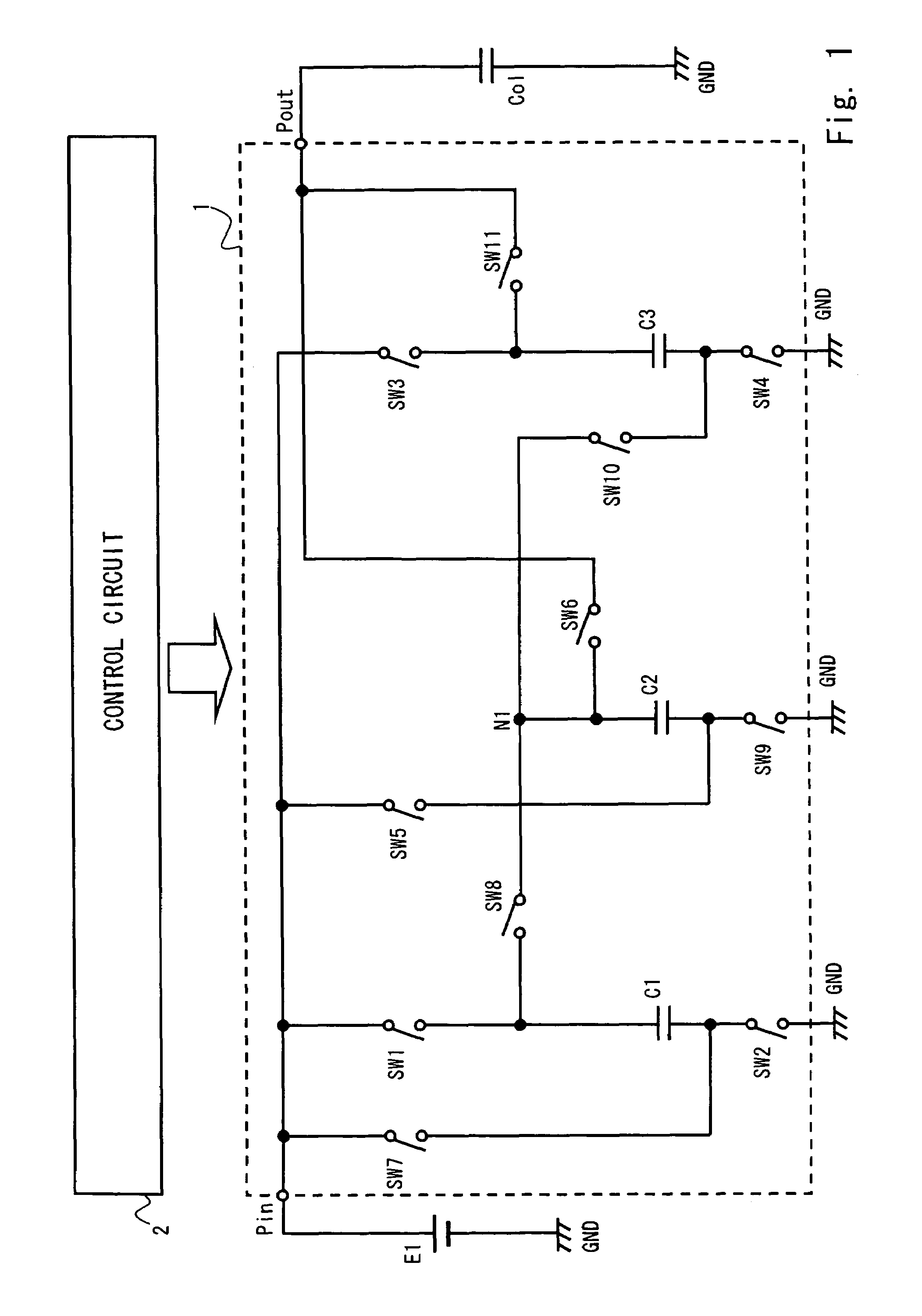
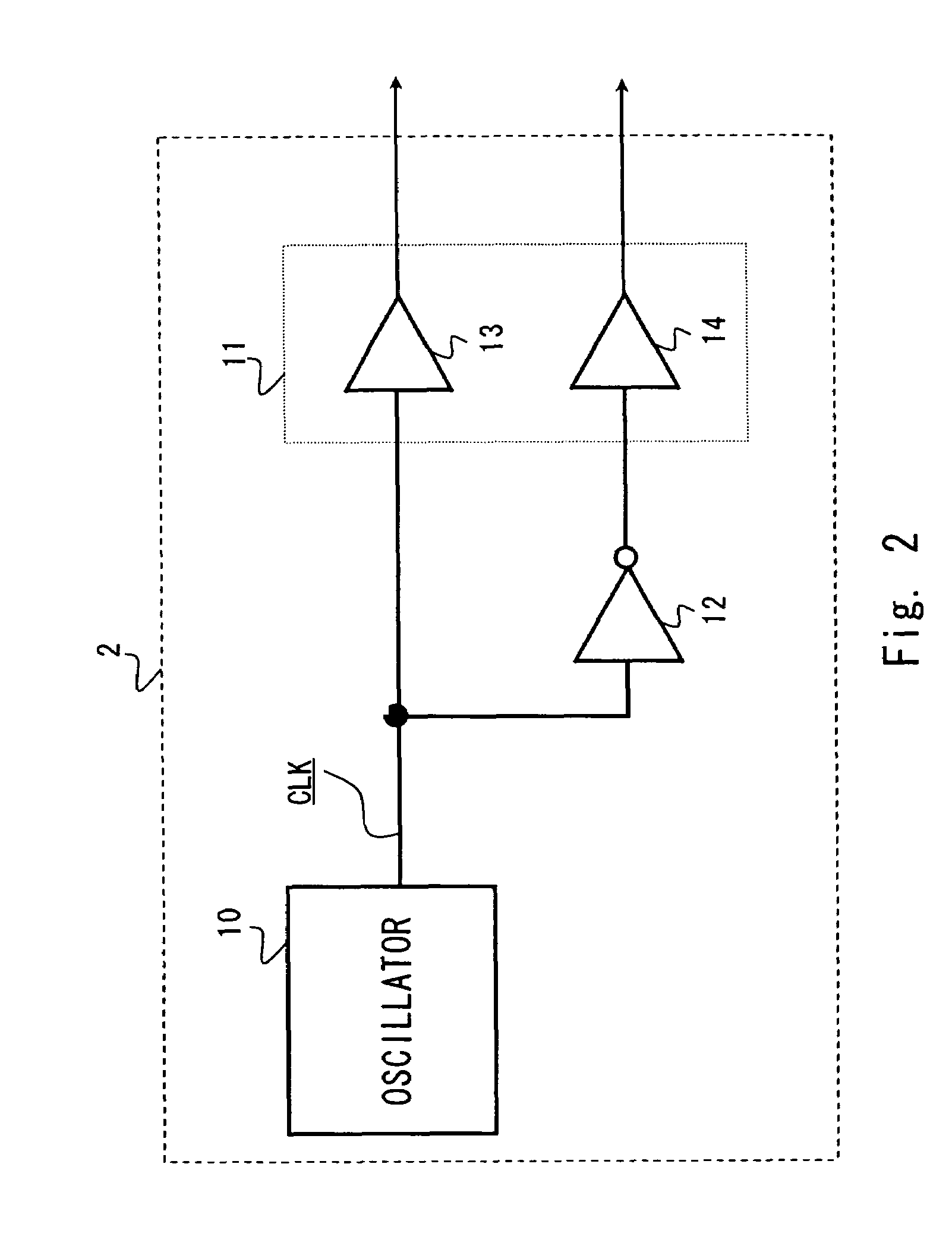
[0025]FIG. 1 shows a schematic circuit diagram of a booster circuit 1 according to the first embodiment of the present invention. A control circuit 2 is also shown in FIG. 1 which controls switches SW1-SW11 ON or OFF. The switches SW1-SW11 are included in the booster circuit 1.

[0026]First, connection relations of circuit elements included in the booster circuit 1 is explained.

[0027]As shown in FIG. 1, the booster circuit 1 includes an input terminal Pin, an output terminal Pout, switches SW1-SW11, and capacitors C1-C3.

[0028]The input terminal Pin is connected to a power supply E1. The output terminal Pout is connected to a smoothing capacitor Col. An input voltage is supplied from the power supply E1 to the booster circuit 1 via the input terminal Pin. The smoothing capacitor Col is charged by an output voltage output from the booster circuit 1 via the output terminal Pout. The output voltage is a voltage gained by boosting the input voltage by the booster circuit 1.

[0029]A first en...

second embodiment

[0070]A booster circuit 20 according to a second embodiment is shown in FIG. 8. The booster circuit 20 is an example of applying this invention to a booster circuit for a negative power supply. The booster circuit 20 outputs an output voltage −2VDD by doubling an input voltage VDD to a negative side. Charging the capacitors C1 and C3 are conducted at a ground potential GND with the power supply E1 as a standard. Charging the capacitor C2 is conducted with a bias between GND-VC1 (VC1 is a potential at one terminal of the capacitor C1). Configuration and operation of the booster circuit 20 are the same with the booster circuit 1 of the first embodiment. Note that in this second embodiment, the ground potential GND is the first power supply potential and the power supply potential VDD is the second power supply potential.

[0071]This invention is not limited to the above mentioned embodiments. That is, it is not limited to a circuit configuration for the three times boosting. It is possi...


PUM


Abstract

A charge pump type booster circuit generates a positive or negative boosted output voltage by switching booster paths one by one. This charge pump type booster circuit includes a plurality of booster paths, each of the plurality of booster paths including at least one booster capacitor, wherein a number of the booster capacitor at each of the plurality of booster paths is different between one booster path and the other booster path. This makes it possible to suppress an increase in a number of an external capacitor for setting an output voltage of the booster circuit constant.

Description

BACKGROUND OF THE INVENTION[0001]1. Field of the Invention[0002]The present invention relates to a booster circuit. More particularly, this invention relates to a charge pump type booster circuit.[0003]2. Description of Related Art[0004]Generally, a booster circuit is required to keep an output voltage constant. However, in a charge pump type booster circuit, the output voltage drops in a relatively short period of time when a value of a current flowing to a load becomes larger. Note that the load is connected to the booster circuit in general.[0005]A related technique disclosed in a Japanese Unexamined Patent Application Publication No. 8-149802 is shown in FIG. 9. As shown in FIG. 9, a booster circuit 100 has two booster units 110, 120. Control signals A and B are input to the booster unit 110. The control signals A and B are input to the booster unit 120 after inverted by buffers, which are connected to input terminals of the booster unit 120. A capacitor C100 is charged by the b...

Claims


Application Information

Patent Timeline
Patent Type & Authority Patents(United States)
IPC IPC(8): G05F1/10G05F3/02
CPCH02M3/07H02M2003/071H02M3/071
Inventor FUJIWARA, HIROFUMI
Owner RENESAS ELECTRONICS CORP
Why Eureka
Try Eureka