Optimizing circuit layouts by configuring rooms for placing devices

a technology of optimizing circuit layout and configuring rooms, applied in the field of circuit layout, can solve the problems of imposing restrictions on the distance between various devices, adversely affecting the electrical behavior of the circuit, and difficult to precisely implement by hand constraints such as matching, symmetry and design rules

Inactive Publication Date: 2010-02-16
CADENCE DESIGN SYST INC
View PDF33 Cites 27 Cited by
  • Summary
  • Abstract
  • Description
  • Claims
  • Application Information

AI Technical Summary

Benefits of technology

[0020]In this way the present invention enables improved methods and systems for opt

Problems solved by technology

Further, the resistances and capacitances introduced by these wires can adversely affect the electrical behavior of the circuit, and these effects need to be minimized as well.
This further imposes restrictions on the distances between various devices in the layout.
Some constraints like matching, symmetry and design rules, however, are very difficult to precisely implement by hand.
Further, since there are a large number of possible arrangements of devices in a layout, it can be very difficult to analyze the impact of multiple tradeoffs between ob

Method used


Image

  • Optimizing circuit layouts by configuring rooms for placing devices
  • Optimizing circuit layouts by configuring rooms for placing devices
  • Optimizing circuit layouts by configuring rooms for placing devices

Examples


Embodiment Construction

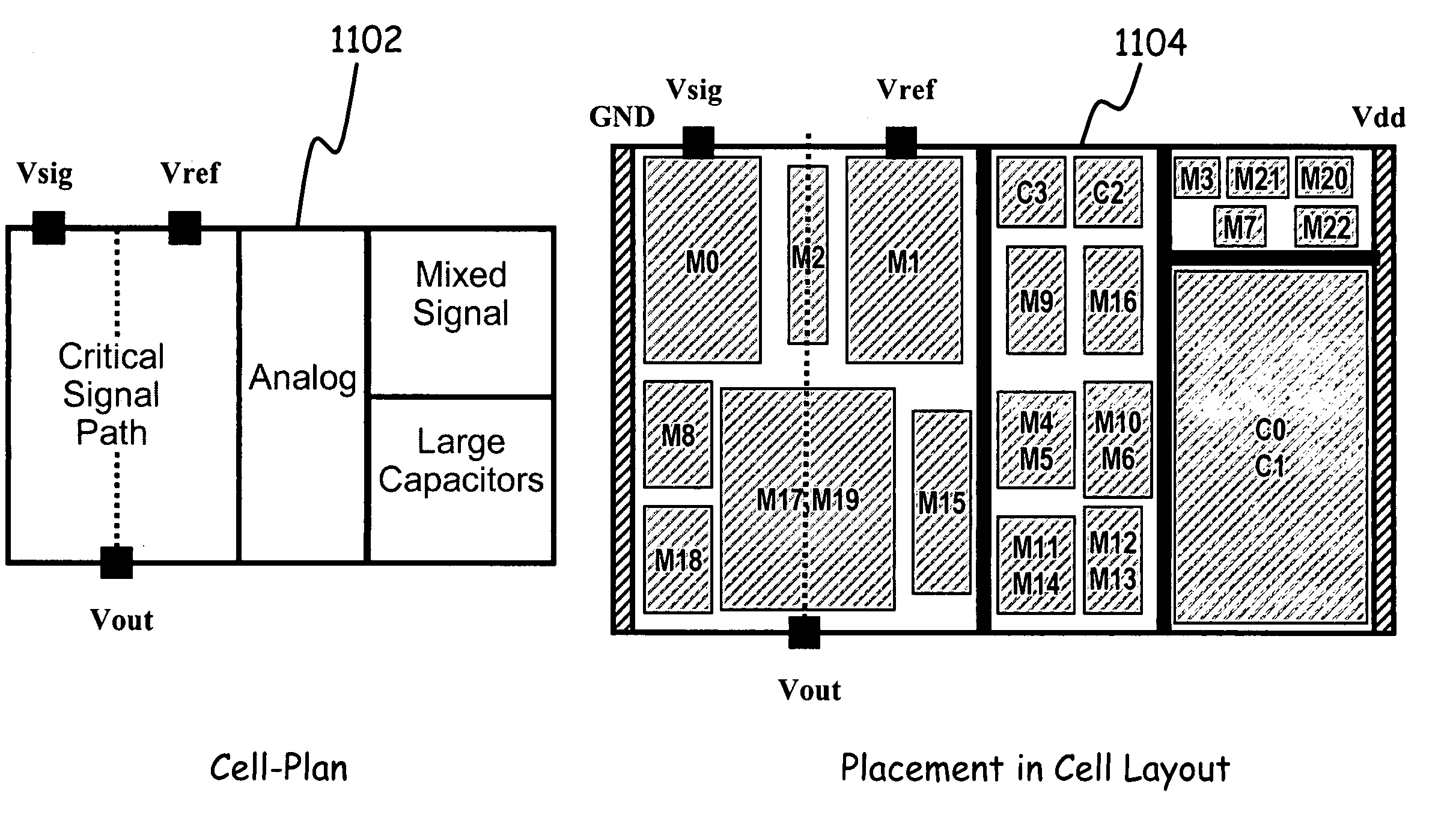
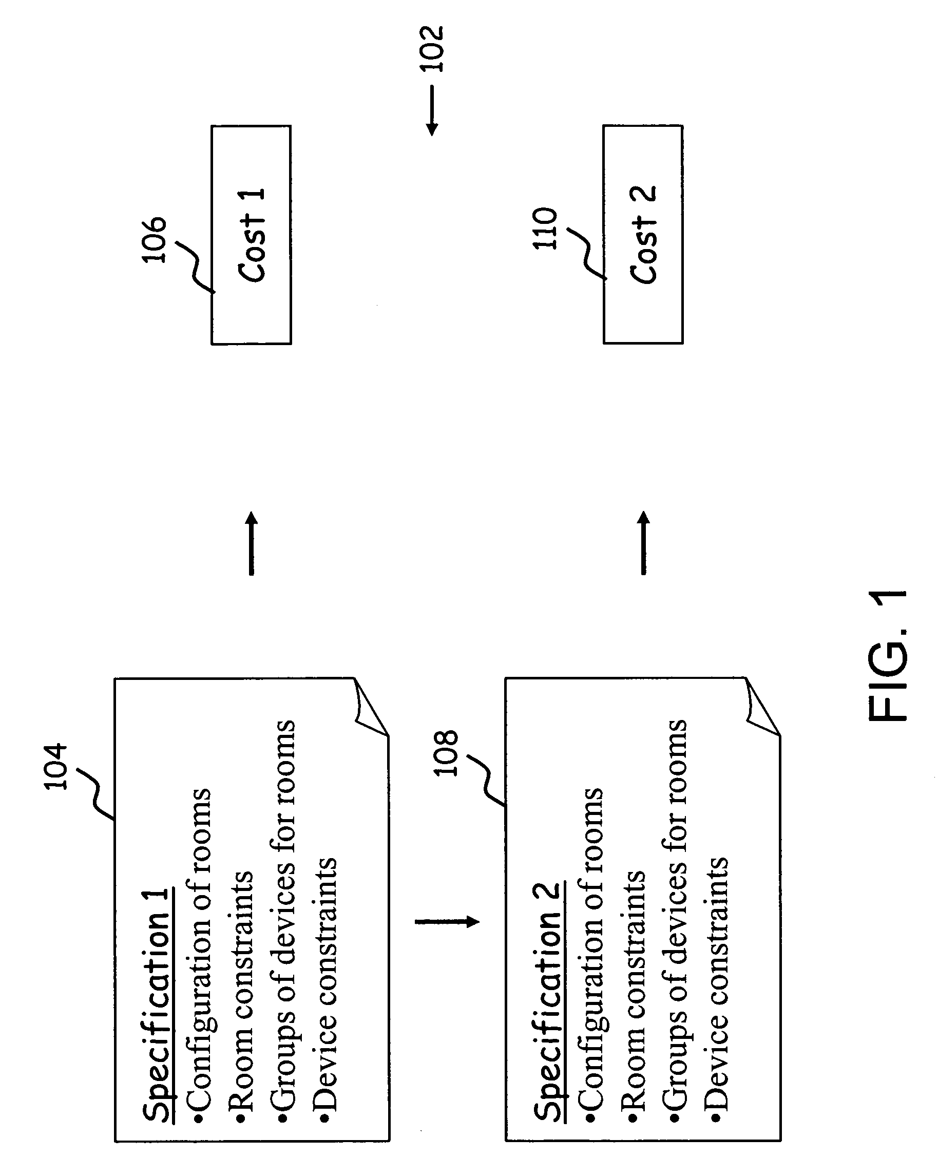
[0039]An embodiment of the present invention is shown in FIG. 1. A method 102 for optimizing a circuit layout includes determining a first layout specification 104 that includes a configuration of rooms for placing devices, one or more room constraints for the configuration of rooms, one or more groups of devices for the rooms, and one or more device constraints for devices in the same room. More specific examples of a specification 104 are discussed below to illustrate arrangements that include constraints on rooms and devices for a circuit layout with particular focus on analog and RF (radio frequency) layouts although other applications are possible. A first cost value 106 measures one or more optimization criteria such a path length, area, or gain. Next a second specification 108 is determined possibly by some adjustment or perturbation of the first specification 104 and a corresponding second cost value 110 is determined for comparison with the first cost value 106. This proces...


PUM


Abstract

A computer-readable medium stores a specification for a circuit layout. The specification includes: a configuration of rooms for placing devices, one or more room constraints for the configuration of rooms, one or more groups of devices for the rooms, and one or more device constraints for devices in a same room. The configuration of rooms may include a tree-structure for the rooms. The room constraints may include a common symmetry line for a first room and a second room. The device constraints may include a self-symmetry constraint for a first device about a symmetry line in a first room. The device constraints may include a symmetry constraint for a first device and a second device about a symmetry line in a first room. The devices may include analog or RF (radio frequency) devices.

Description

BACKGROUND OF THE INVENTION[0001]The present invention relates generally to circuit layouts and more particularly to optimizing circuit layouts for analog and RF (radio frequency) circuits.[0002]Circuit design for analog and RF circuits poses a number of unique challenges. In order for a circuit to perform correctly when manufactured using a semi-conductor process, several techniques have been employed when positioning devices (i.e., analog and RF devices) in the layout.[0003]For example, a common technique involves matching the ratios of sizes, orientations and other properties between one or more devices in order to achieve electrical equivalence between these devices when manufactured. Additionally, in order to minimize the influence of process variations, certain groups of devices are placed in close proximity to each other. Another common matching technique involves positioning devices “symmetrically” by mirroring their orientations and usually aligning them in one dimension an...

Claims


Application Information

Patent Timeline
IPC IPC(8): G06F17/50
CPCG06F30/392
Inventor GOPALAKRISHNAN, PRAKASHYUROVSKY, ALISA
Owner CADENCE DESIGN SYST INC
Why Eureka
Try Eureka