Flip-chip semiconductor device with improved power pad arrangement

a technology of flip-chip semiconductors and power pads, applied in semiconductor devices, semiconductor/solid-state device details, electrical equipment, etc., can solve the problems of reducing the number of signal pads, affecting the performance of the device, so as to reduce the difference in circuit delay

Inactive Publication Date: 2009-10-13
RENESAS ELECTRONICS CORP
View PDF7 Cites 4 Cited by
  • Summary
  • Abstract
  • Description
  • Claims
  • Application Information

AI Technical Summary

Benefits of technology

[0038]Such arrangement causes interconnection resistances from pads to the power supply interconnection to be symmetrical, and thereby allows distribution of the potential drop to be symmetrical with respect to the symmetry line. This effectively reduces the circuit delay difference caused by different potential drops.

Problems solved by technology

The increase in the number of signal pads may cause a problem, because conventional quad flat packaging (QFP) and pin grid array packaging (PGA) may not provide a required number of signal terminals.
In such a flip-chip semiconductor device, the peripheral portion of the internal area experiences potential drop of power supply lines, most severely.
Such structure undesirably suffers from increased difference in the interconnection resistance caused by the difference in the interconnection structure difference depending on the positions over the semiconductor chip.
This may cause a problem that potential drops along the power supply interconnections are largely different between portions near the top / bottom edges and portions near the right / left edges.
This is undesirable for satisfying operation requirements of the semiconductor device.
Jp-2000 277656A discloses a multi-level printed circuit board having interconnections arranged in a symmetrical manner; however, this document does not disclose pad and interconnection arrangement of a flip-chip semiconductor device.

Method used


Image

  • Flip-chip semiconductor device with improved power pad arrangement
  • Flip-chip semiconductor device with improved power pad arrangement
  • Flip-chip semiconductor device with improved power pad arrangement

Examples


first embodiment

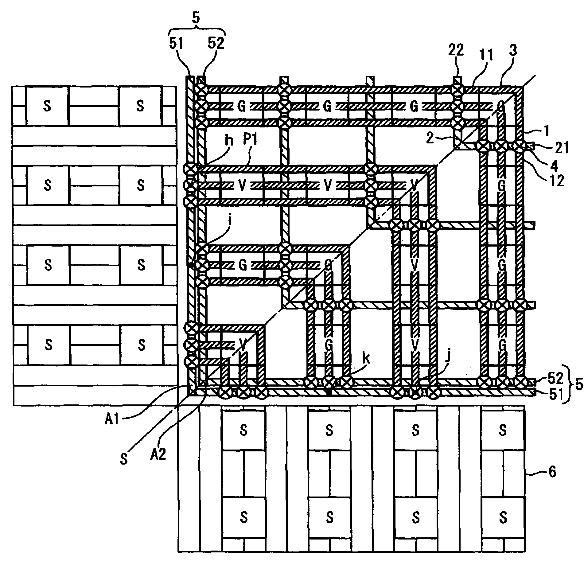
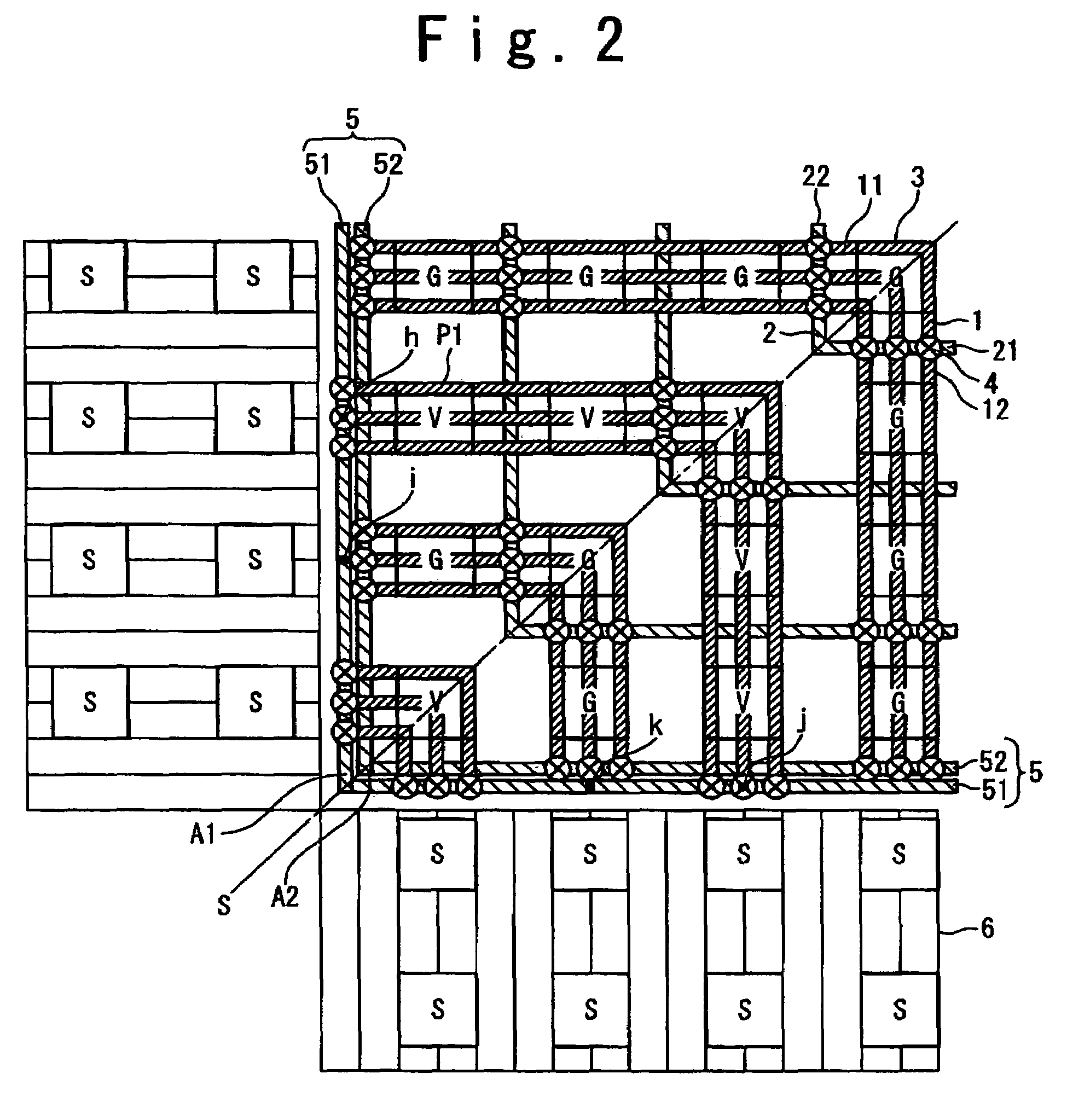
[0047]FIG. 2 illustrates an arrangement of power pads and interconnections within a flip-chip semiconductor device in a It should be noted that FIG. 2 partially illustrates the structure of the flip-chip semiconductor device in this embodiment; FIG. 2 only illustrates a one-fourth portion at the lower left of the entire flip-chip semiconductor device. The lower right, upper left and upper right portions of the semiconductor device are correspondingly configured in the right-to-left symmetry and in the top-to-bottom symmetry. These portions are not shown in FIG. 1.

[0048]The flip-chip semiconductor device in this embodiment is composed of first-level interconnections 1, second-level interconnections 2, power pads 3, via contacts 4, and chip peripheral power supply loops 5 within the internal area surrounded by an I / O region

[0049]The first-level interconnections 1 are integrated within the uppermost interconnection level of the semiconductor device. In the following, horizontally-exte...

third embodiment

[0085]FIG. 4 illustrates an exemplary arrangement of a flip-chip semiconductor device in a In the arrangement shown in FIG. 4, the first-level interconnections 1 are arranged not to cross the power pads 3. It should be noted that the FIG. 4 only illustrates the lower left portion of the semiconductor device. It should be also understood that an I / O region 6 is also provided around the internal area in this embodiment although not shown in FIG. 4.

[0086]In the third embodiment, the first-level interconnections 1 are arranged passing between adjacent power pads 3. The power pads 3 are connected with the first-level interconnections 1 through branch interconnections. The branch interconnections branching from the first-level horizontal interconnections 11 are referred to as the branch interconnections 111, and the branch interconnections branching from the first-level vertical interconnections 12 are referred to as the branch interconnections 121. In this embodiment, the branching inte...

fourth embodiment

[0090]In the fourth embodiment, the first-level interconnections 1 are paired, passing between the power pads 3. One of each paired first-level interconnections 1 is connected to the VDD pads, and the other is connected to the GND pads. In this embodiment, the VDD pads and the GND pads are connected with the associated first-level interconnections 1 through branching interconnections 111, 121.

[0091]As shown in FIG. 6, the second-level interconnections 2 are arranged identically to the arrangement in FIG. 2, except for that the second-level interconnections 2 are paired. Referring back to FIG. 5, one of the paired second-level interconnections 2 is connected with the first-level interconnections 1 connected with the VDD pads, and the other is connected with the first-level interconnections 1 connected with the GND pads.

[0092]It would be apparent that the arrangement shown in FIG. 5, in which the power pads 3, the first-level interconnections 1, the second-level interconnections 2, an...


PUM


Abstract

A semiconductor device is composed of a power supply interconnection extending from a certain starting point in a first direction and also extending from the starting point in a second direction orthogonal to the first direction, a plurality of power pads, and connecting interconnections providing electrical connection between the power supply interconnection and the power pads. The power supply interconnection, the power pads, and the connecting interconnections are arranged in a symmetrical manner with respect to a symmetry line crossing the starting point and extending in a direction at an angle of 45 degree to the first and second directions.

Description

BACKGROUND OF THE INVENTION[0001]1. Field of the Invention[0002]The present invention relates to flip-chip semiconductor devices, particularly to power / ground pad arrangement of flip-chip semiconductor devices.[0003]2. Description of the Related Art[0004]With the improvement of the fine processing technology, semiconductor devices which have been conventionally integrated within plural separate chips can be integrated within a single semiconductor chip.[0005]This is, however, accompanied by the increase in a total number of signal terminals of the single semiconductor chip. The increase in the number of signal pads may cause a problem, because conventional quad flat packaging (QFP) and pin grid array packaging (PGA) may not provide a required number of signal terminals. Accordingly, the flip-chip packaging technique has been increasingly used, instead of the QFP and PGA techniques.[0006]Flip chip packages have various advantages. Firstly, total numbers of signal terminals can be inc...

Claims


Application Information

Patent Timeline
Patent Type & Authority Patents(United States)
IPC IPC(8): H01L23/52
CPCH01L23/5286H01L24/06H01L2924/3011H01L2924/14H01L2924/00
Inventor KATOU, TOSHIKAZU
Owner RENESAS ELECTRONICS CORP
Why Eureka
Try Eureka