Method for forming PECVD silicon nitride film
a silicon nitride film and pecvd technology, applied in the direction of crystal growth process, polycrystalline material growth, semiconductor/solid-state device testing/measurement, etc., can solve the problems of reducing the overall manufacturing yield, and reducing the deposition rate of each batch of wafers, so as to achieve the effect of improving yield
- Summary
- Abstract
- Description
- Claims
- Application Information
AI Technical Summary
Benefits of technology
Problems solved by technology
Method used
Image


Examples
Embodiment Construction
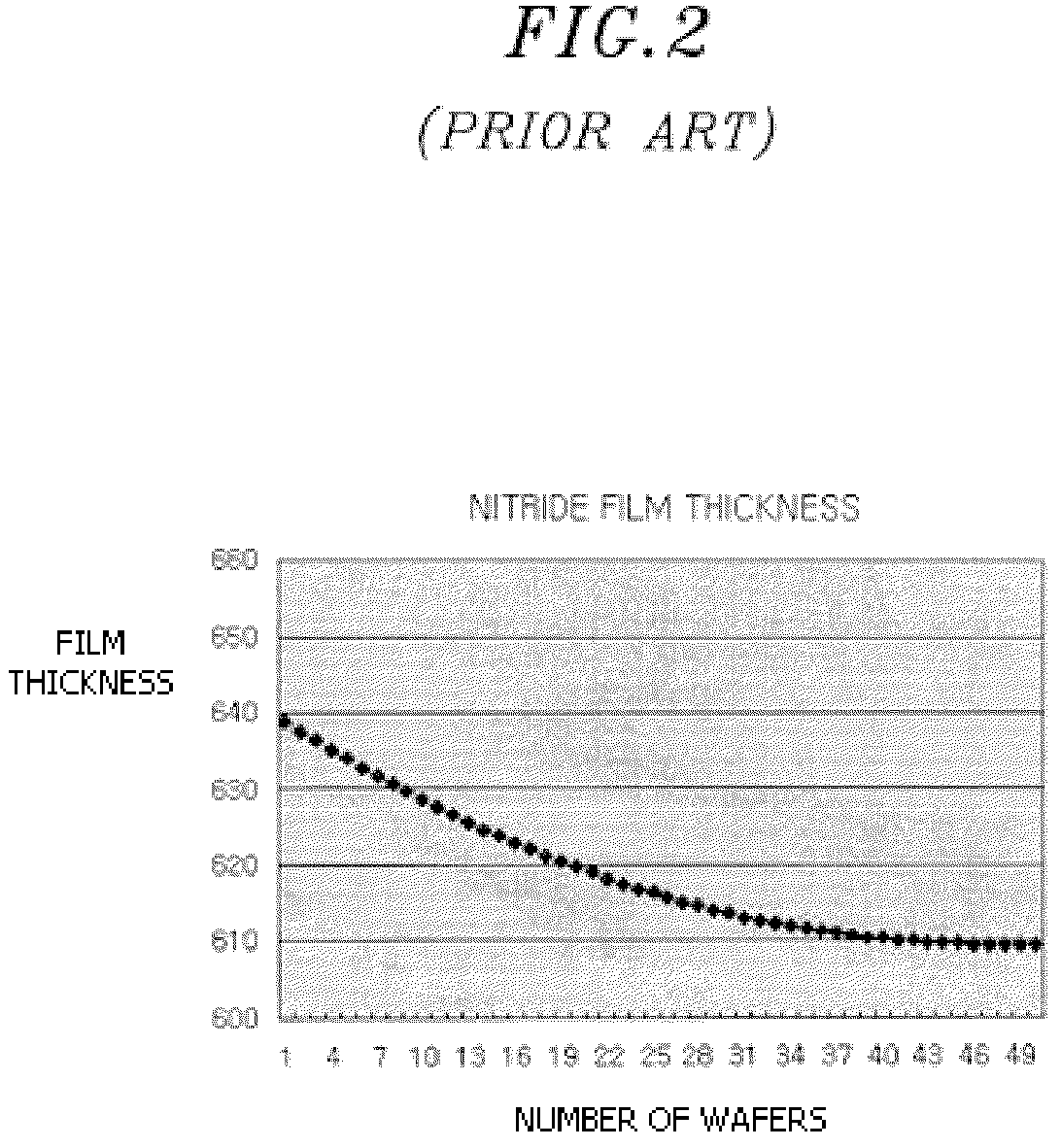
[0013]In general, example embodiments of the invention relate to forming a silicon nitride film in a PECVD chamber. In one example embodiment, a method for forming a silicon nitride film in a PECVD chamber can improve yield by maintaining a uniform thickness of silicon nitride films across different batches of processed wafers despite temperature variations introduced by an RF plasma cleaning process.
[0014]In accordance with one example embodiment of the present invention, a method for forming a silicon nitride film in a PECVD chamber includes pre-coating the PECVD chamber with a silicon nitride film to form a protection layer, inserting a wafer into the PECVD chamber to deposit a silicon nitride film on the wafer, and cleaning the PECVD chamber with RF plasma after depositing the silicon nitride film on a predetermined number of wafers. The time for depositing the silicon nitride film in the PECVD chamber is adjusted so as to deposit the silicon nitride film with a uniform thicknes...
PUM
| Property | Measurement | Unit |
|---|---|---|
| thickness | aaaaa | aaaaa |
| deposition time | aaaaa | aaaaa |
| time | aaaaa | aaaaa |
Abstract
Description
Claims
Application Information
 - R&D
- Intellectual Property
- Life Sciences
- Materials
- Tech Scout
- Unparalleled Data Quality
- Higher Quality Content
- 60% Fewer Hallucinations
Browse by: Latest US Patents, China's latest patents, Technical Efficacy Thesaurus, Application Domain, Technology Topic, Popular Technical Reports.
© 2025 PatSnap. All rights reserved.Legal|Privacy policy|Modern Slavery Act Transparency Statement|Sitemap|About US| Contact US: help@patsnap.com