Buried via technology for three dimensional integrated circuits

a technology of integrated circuits and vias, applied in the field of integrated circuits, can solve the problems of difficult and inefficient combination with state of the art 2-dimensional circuit technologies, and the problem of blocking this power routing layer,

Inactive Publication Date: 2010-03-02
TELEDYNE SCI & IMAGING
View PDF31 Cites 199 Cited by
  • Summary
  • Abstract
  • Description
  • Claims
  • Application Information

AI Technical Summary

Problems solved by technology

This creates exclusion area constraints that make combination with state of the art 2-dimensional circuit technologies difficult and inefficient.
Blocking this power routing layer is problematic.

Method used


Image

  • Buried via technology for three dimensional integrated circuits
  • Buried via technology for three dimensional integrated circuits
  • Buried via technology for three dimensional integrated circuits

Examples


Embodiment Construction

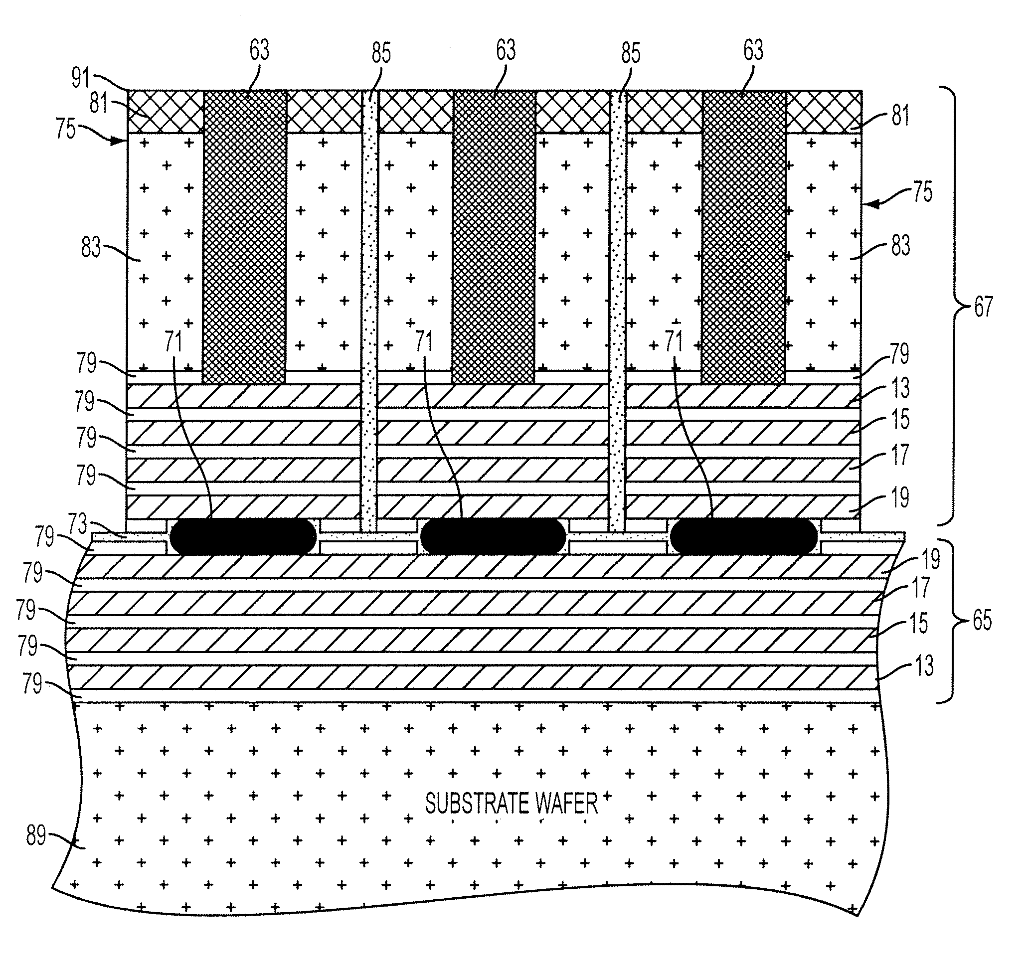
[0026]An apparatus and method is provided herein for a buried via in three dimensional integrated circuits. The buried via does not interrupt the routing at all metal layers and avoids full penetration of the wafer. The buried via may be used to interconnect between metal layers on adjacent active circuit layers from separate dies or wafers with no or less exclusion area constraints as compared to a through via interconnect. As a result, the apparatus and method provided herein allow improved electrical interconnects of three dimensional integrated circuits with state of the art IC technologies.

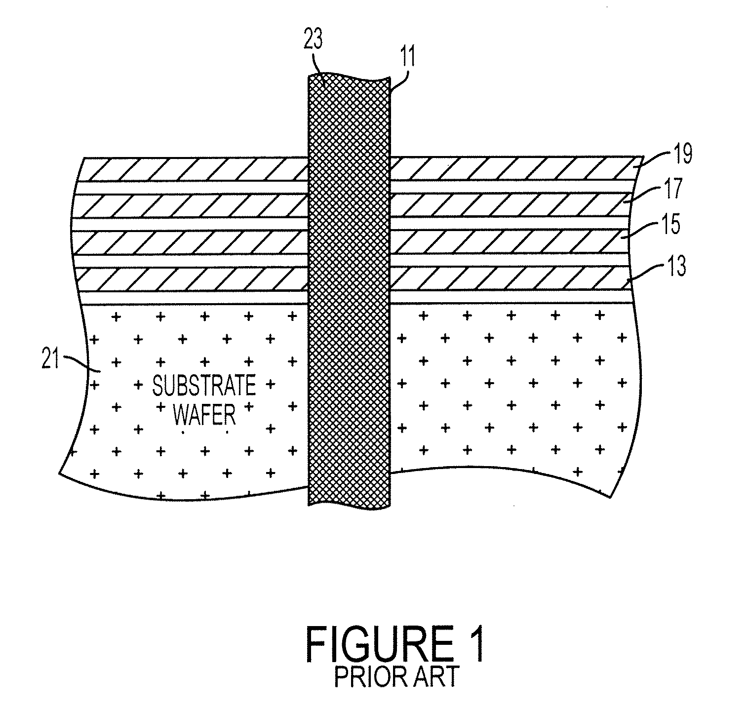
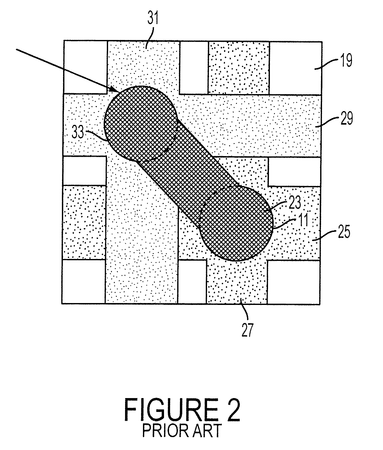
[0027]FIG. 3 is a cross sectional view of a three dimensional integrated circuit 35 with a buried via 59, according to an embodiment of the invention. The three dimensional integrated circuit 35 has three layers: a first active circuit layer 36, a second active circuit layer 37 and a third active circuit layer 38. A bond material 56, such as indium, gold or solder, may be used to couple the f...


PUM

PropertyMeasurementUnit
thickaaaaaaaaaa
aspect ratioaaaaaaaaaa
thickaaaaaaaaaa

Abstract

A three dimensional integrated circuit and method for making the same. The three dimensional integrated circuit has a first and a second active circuit layers with a first metal layer and a second metal layer, respectively. The metal layers are connected by metal inside a buried via. The fabrication method includes etching a via in the first active circuit layer to expose the first metal layer without penetrating the first metal layer, depositing metal inside the via, the metal inside the via being in contact with the first metal layer, and bonding the second active circuit layer to the first active circuit layer using a metal bond that connects the metal inside the via to the second metal layer of the second active circuit layer.

Description

CLAIM OF PRIORITY UNDER 35 U.S.C. § 119[0001]This application claims the benefit of Provisional Application No. 60 / 766,526, filed Jan. 25, 2006, herein incorporated by reference in its entirety.BACKGROUND OF THE INVENTION[0002]1. Field of the Invention[0003]The invention relates generally to integrated circuits. More particularly, the invention relates to buried via technology for three dimensional integrated circuits.[0004]2. Description of Related Art[0005]Three dimensional integrated circuit (IC) technology provides powerful capability for increased IC functionality. The three dimensional IC technology utilizes a multi-layer of active circuitry stacked up one on top of the other. Each active layer may consist of several metal layers with a thickness of about 1 micron each, forming an electric interconnect network between active devices, such as transistors.[0006]To fully exploit three dimensional IC technology, high density vertical interconnects with conductive wiring between st...

Claims


Application Information

Patent Timeline
Patent Type & Authority Patents(United States)
IPC IPC(8): H01L23/02
CPCH01L21/76898H01L25/0657H01L25/50H01L2224/16H01L2225/06513H01L2225/06541H01L2224/05573H01L2224/13025H01L2924/00014H01L2224/05599
Inventor LAUXTERMANN, STEFAN C.DENATALE, JEFFREY F.
Owner TELEDYNE SCI & IMAGING
Why Eureka
Try Eureka