Three-dimensional chip-stack package and active component on a substrate

a three-dimensional chip and active component technology, applied in the direction of cooling/ventilation/heating modification, semiconductor/solid-state device details, semiconductor devices, etc., can solve the problems of insufficient bonding strength, insufficient flexible finished substrate, damage to other components, etc., to achieve less thermo stress

Inactive Publication Date: 2009-01-08
IND TECH RES INST
View PDF20 Cites 46 Cited by
  • Summary
  • Abstract
  • Description
  • Claims
  • Application Information

AI Technical Summary

Benefits of technology

[0011]In view of the foregoing, an objective of the invention is to provide 3D chip-stack package adapted to be

Problems solved by technology

It is likely to damage other components not to be embedded.
The finished substrate is not flexible and has limited applications.
'050 re-distributes the bonding pads by sev

Method used


Image

  • Three-dimensional chip-stack package and active component on a substrate
  • Three-dimensional chip-stack package and active component on a substrate
  • Three-dimensional chip-stack package and active component on a substrate

Examples


second embodiment

[0064]Further, please refer to FIG. 8 which a schematic cross-sectional view of active component on a substrate according to the invention. The structure of active component on a substrate is similar to that in FIG. 7 and comprises a component-embedded plate 70a and a flexible substrate 80. The same elements will not be described again. The differences includes the active component 74a embedded in the dielectric layer 72 is made by a flexible material. The flexible material can be, but not limited to, polymer.

[0065]The component-embedded plate 70a is further stacked by a side IC 79. The side IC 79 has a plurality of conductive pads 790, 791. The pads 790, 791 are electrically connected with the electrical circuit 76. The active component 74a and the side IC 79 have integrated electrical circuits inside for performing specific functions. In addition, the side IC 59 can be a regular IC or an IC with TSVs.

[0066]The side IC 79 can be, but not limited to, made by a flexible material. Acc...

fifth embodiment

[0073]Moving right along, please refer to FIG. 11 which is a schematic cross-sectional view of active component on a substrate according to the invention. According to this embodiment, the active component on a substrate comprises a component-embedded plate 70 and a heat-dissipating substrate 86.

[0074]The component-embedded plate 70 comprises a dielectric layer 72, an active component 74 and an electrical circuit 76. The dielectric layer 72 has a first surface 720, a second surface 722 and a plurality of conductive holes 726, 727. The conductive holes 726, 727 penetrate the dielectric layer 72 and connected between the second surface 722 and the active component 74. The active component 74, dielectric layer 72 and the heat-dissipating substrate 86 are bendable and flexible for flexible electronics. The heat-dissipating substrate 86 is contact with both the exposed surface of the active component 74 and the first surface 720 for dissipating heat generated by the active component 74. ...


PUM


Abstract

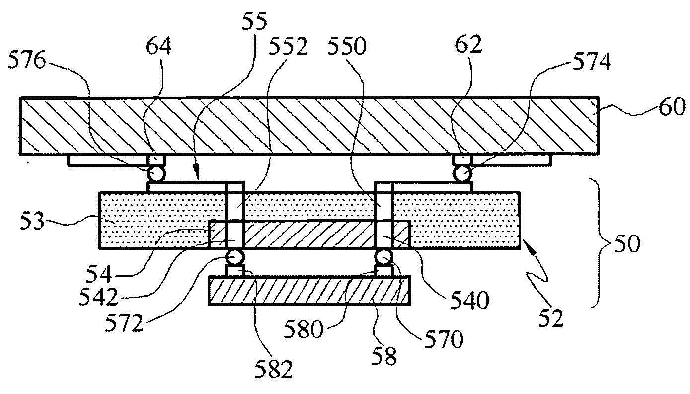
The 3D chip-stack package comprises a component-embedded plate and a side IC. The PCB has a plurality of conductive contacts. The component-embedded plate comprises a dielectric layer; an active component embedded in the dielectric layer, one surface of each active component exposed outside the dielectric layer, the active components having a plurality of TSVs (Through Silicon Via), one ends of the TSVs exposed outside the exposed surface, the other ends of the TSVs corresponding to the conductive contacts of the PCB; and an electrical circuit on the dielectric layer and in electrical connection between the other ends of the TSVs of the active component and the corresponding conductive contacts of the PCB, respectively. The side IC has a plurality of pads. The pads are electrically connected with the exposed ends of the TSVs of the active component.

Description

[0001]The present application is a continuation-in-part of parent application Ser. No. 11 / 252,572, filed Oct. 19, 2005, which claims the benefit of Taiwan Patent Application No. 093135743, filed on Nov. 19, 2004. The parent application and the Taiwan application are hereby incorporated by reference for all purposes as if fully set forth herein.BACKGROUND[0002]1. Field of Invention[0003]The invention relates to a three-dimensional (3D) chip-stack package structure. In particular, it relates to a structure of embedded active components having TSVs (through silicon via).[0004]2. Related Art[0005]In order to create larger space and to enhance the functions of the module within a limited substrate area, shrunk or embedded passive components are often used to minimize the circuit layout and to reduce the signal transmission distance. Thus, more space is left for installing active components and enhancing the overall performance. Therefore, substrates with passive components such as embedd...

Claims


Application Information

Patent Timeline
IPC IPC(8): H01L23/538H05K7/20
CPCH01L21/561H01L2924/18162H01L21/6835H01L23/49816H01L23/5389H01L24/19H01L24/96H01L24/97H01L25/0657H01L2221/68345H01L2224/04105H01L2224/16H01L2224/20H01L2224/211H01L2224/97H01L2225/06513H01L2225/06541H01L2924/01029H01L2924/01075H01L2924/14H01L2924/15311H01L2924/15331H01L2924/19041H01L2924/19042H01L2924/19043H01L2924/3511H01L21/568H01L2224/12105H01L2224/0401H01L2224/8203H01L2924/01033H01L2924/01087H01L2224/82H01L2224/13025H01L2224/16145H01L2224/16225H01L2224/73259H01L2225/1035H01L2225/1058H01L2924/15788H01L2924/00
Inventor KO, CHENG-TALU, SU TSAI
Owner IND TECH RES INST
Why Eureka
Try Eureka