Microelectromechanical system based sensors, sensor arrays, sensing systems, sensing methods and methods of fabrication

a microelectromechanical system and sensor array technology, applied in the direction of fluid pressure measurement, coupling device connection, instruments, etc., can solve the problems of low reliability, high cost of side-mounted imaging array assembly process, and limited free-space chip-to-chip optical interconnect based on two-dimensional cmos imaging array and surface-emitting laser array, etc., to improve the manufacturability of the sensor, improve the flexibility of the design of the optical communication system, and reduce the fabrication cost of the sensor array

Inactive Publication Date: 2005-01-18
XEROX CORP
View PDF21 Cites 54 Cited by
  • Summary
  • Abstract
  • Description
  • Claims
  • Application Information

AI Technical Summary

Benefits of technology

The systems and methods according to this invention separately provide improved flexibility in the design of an optical communication system for semiconductor chips.
The systems and methods according to this invention separately provide reduced fabrication costs of a sensor or sensor array for a semiconductor chip.
The systems and methods according to this invention separately provide improved manufacturability of a sensor or sensor array for a semiconductor chip.
The systems and methods according to this invention separately provide increased reliability of a sensor or sensor array for a semiconductor chip.
The systems and methods according to this invention separately provide chip-to-chip communication with improved robustness and / or reliability.

Problems solved by technology

The conventional sensor arrays for chip-to-chip communication have various limitations and drawbacks.
For example, the free-space chip-to-chip optical interconnect based on two-dimensional CMOS imaging arrays and surface-emitting laser arrays is limited to vertically stacked chips.
Further, the assembly process of side-mounted imaging arrays is costly and has low reliability.

Method used


Image

  • Microelectromechanical system based sensors, sensor arrays, sensing systems, sensing methods and methods of fabrication
  • Microelectromechanical system based sensors, sensor arrays, sensing systems, sensing methods and methods of fabrication
  • Microelectromechanical system based sensors, sensor arrays, sensing systems, sensing methods and methods of fabrication

Examples


Embodiment Construction

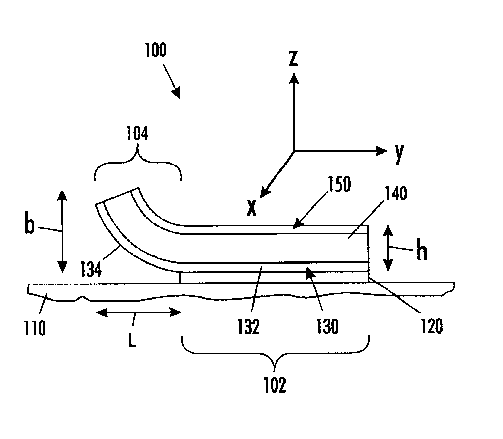
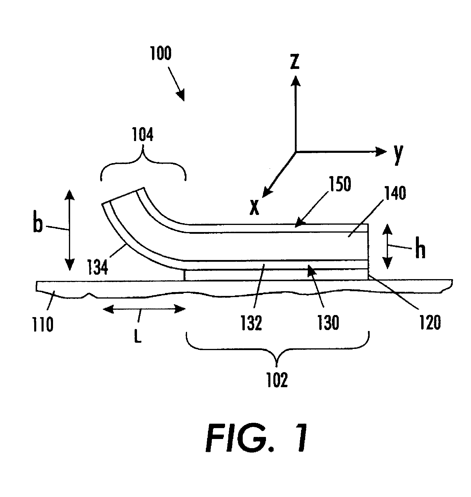
While the invention is described hereafter with reference to various systems that incorporate one or more sensors according to this invention, it should be understood that this invention is not strictly limited to such systems. Rather, any microelectromechanical system (MEMS) based system that utilizes a sensor is contemplated by this invention. The description is intended to convey the features of the invention without limiting the invention to the specific embodiments disclosed.

Furthermore, while various details of methods of fabricating a sensor according to this invention are described, it should be understood that this invention is not strictly limited to such methods. Rather, any known or hereafter developed microelectromechanical system (MEMS) based fabrication techniques may be used. For example, known techniques for forming stress-engineered or stress gradient-induced structures such as spring contacts, coils and / or suspension arms may be used. In particular, various suitab...


PUM


Abstract

A microelectromechanical system (MEMS) based sensor comprises: a substrate defining a plane; a first conductive material layer having a first stress, a first portion of the first conductive material layer being connected to the substrate and extending in a substantially parallel direction to the plane defined by the substrate and a second portion being disconnected from the substrate and extending in a substantially non-parallel direction to the plane defined by the substrate; and a sensor material layer formed over at least the second portion of the first conductive material layer, the sensor material layer having a second stress that is less than the first stress of the first conductive material layer. The stresses form a stress gradient that bends the second portion of the first conductive material layer and the sensor material layer formed over the second portion of the first conductive material layer away from the substrate.

Description

BACKGROUND OF THE INVENTION1. Field of InventionThis invention relates to microelectromechanical system (MEMS) based structures and microelectromechanical system (MEMS) based systems including at least one sensor.This invention also relates to methods for fabricating such structures and systems, as well as methods for sensing using such microelectromechanical system based systems.2. Description of Related ArtConventional sensor arrays that allow communication between integrated circuit chips are built into chips parallel to the substrate. For example, a typical free-space chip-to-chip optical interconnect may be based on two-dimensional CMOS imaging arrays and surface-emitting laser arrays. The two-dimensional CMOS imaging arrays are flip-chip bonded onto a semiconductor chip. The surface-emitting laser arrays are flip-chip bonded onto a separate semiconductor chip. The two-dimensional CMOS imaging arrays are then aligned with the surface-emitting laser arrays by vertically stacking...

Claims


Application Information

Patent Timeline
Patent Type & Authority Patents(United States)
IPC IPC(8): H01L21/00H01L23/48H01R11/22H01R11/11B81B3/00
CPCB81B3/0021B81B2201/0292B81B2201/038H01R9/096B81B2203/0118B81C2201/0167B81B2201/047H01R12/52
Inventor MEI, PINGSUN, DECAISTREET, ROBERT A.
Owner XEROX CORP
Why Eureka
Try Eureka