Access Transistor of a Nonvolatile Memory Device and Method for Fabricating Same

a nonvolatile memory device and access transistor technology, applied in the direction of semiconductor devices, basic electric elements, electrical appliances, etc., can solve the problems of reducing the effective chip area pet of data bit without, and the challenges of designing, fabricating, and operating vertical nand flash memory devices

Active Publication Date: 2016-08-11
MOSAID TECH
View PDF6 Cites 46 Cited by
  • Summary
  • Abstract
  • Description
  • Claims
  • Application Information

AI Technical Summary

Problems solved by technology

But as fabrication process limitations (for example, limitations imposed by photolithography tools) limit the ability to reduce physical transistor sizes, there have been structural and / or design schemes proposed to increase memory density, such as, for example, stacking NAND cells in a direction perpendicular to the chip surface, thereby reducing the effective chip area pet: data bit without requiring shrinkage of the physical cell transistor size.
However, there continue to be challenges associated with designing, fabricating, and operating vertical NAND flash memory devices.

Method used


Image

  • Access Transistor of a Nonvolatile Memory Device and Method for Fabricating Same
  • Access Transistor of a Nonvolatile Memory Device and Method for Fabricating Same
  • Access Transistor of a Nonvolatile Memory Device and Method for Fabricating Same

Examples


Embodiment Construction

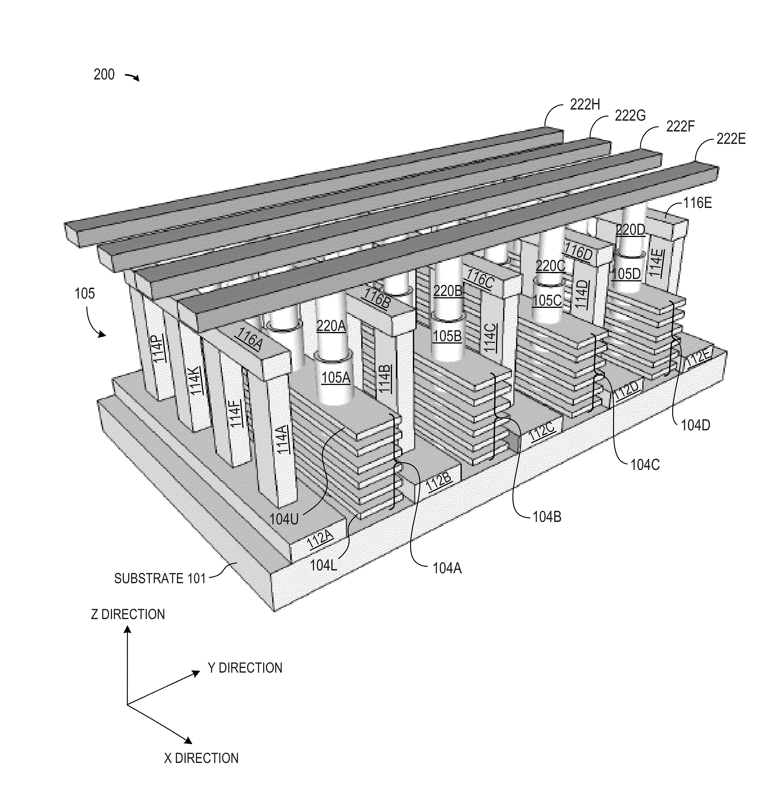
[0025]In three-dimensional vertical channel nonvolatile memory device, a stacked memory architecture and cell array structure are provided having select transistors with elevated substrate layers to form extended source line regions to provide improved turn-off characteristics for the select transistors. In selected embodiments, the elevated substrate layers are formed with epitaxial semiconductor strips which extend in the word line direction on both sides of a around select access transistor gate electrode and separated therefrom by an insulating gate dielectric layer. Each epitaxial semiconductor strip may have at least a portion formed with a specified doping type (e.g., n-type) or a highly doped conductive or silicide upper source region to define a source region which is positioned in overlap with the ground select access transistor gate electrode. By connecting the flash cell strings between the upper connection bit lines and an n-type elevated source region protruding from t...


PUM


Abstract

A three-dimensional integrated circuit nonvolatile memory array includes a memory array of vertical channel NAND flash strings connected between an upper layer connection bit line and a substrate which includes one or more elevated source regions disposed on at least one side of each row of NAND flash strings so that each NAND flash string includes a lower select transistor with a first channel portion that runs perpendicular to the surface of the substrate through a vertical channel string body, a second channel portion that runs parallel to the surface of the substrate, and a third channel portion that runs perpendicular to the surface of the substrate through the elevated source region.

Description

BACKGROUND OF THE INVENTION[0001]1. Field of the Invention[0002]The present invention is directed in general to integrated circuit devices and methods for manufacturing same. In one aspect, the present invention relates to nonvolatile memory devices, such as NAND flash memory and other types of flash memory.[0003]2. Description of the Related Art[0004]With the increasing demand for nonvolatile data storage in consumer electronics having mass storage, such as video or audio players, digital cameras, and other computerized devices, there continues to be interest in having nonvolatile memory devices progress over time towards having smaller sizes, larger memory capacity, and improved performance. Flash memory is a commonly used type of nonvolatile memory which can take the form of memory cards or USB type memory sticks, each having at least one memory device and a memory controller formed therein. For example, the need to reduce manufacturing costs per data bit is driving the NAND flas...

Claims


Application Information

Patent Timeline
Patent Type & Authority Applications(United States)
IPC IPC(8): H01L27/115
CPCH01L27/11524H01L27/11556H01L27/1157H01L27/11582H10B43/10H10B43/35H10B43/27
Inventor RHIE, HYOUNG SEUB
Owner MOSAID TECH
Why Eureka
Try Eureka