Three-dimensional die stacks with inter-device and intra-device optical interconnect

a technology of optical interconnection and die stack, which is applied in the direction of optical elements, optical waveguide light guides, instruments, etc., can solve the problems of global wires, fundamental limitations in the growth of future silicon based computer systems, and the inability to interconnect transistors in parallel

Active Publication Date: 2011-11-22
HEWLETT-PACKARD ENTERPRISE DEV LP
View PDF18 Cites 46 Cited by
  • Summary
  • Abstract
  • Description
  • Claims
  • Application Information

AI Technical Summary

Problems solved by technology

The growth of future silicon based computer systems is fundamentally limited by the inter-related problems of signal integrity, wire-based global signaling, and thermal properties.
As integrated circuit process technology progressively shrinks transistor sizes, the wires that interconnect the transistors are increasingly becoming a limiting problem.
However, global wires are a problem in high performance systems since, among other factors, they must be driven by large transistors.
This consumes large amounts of power which in turn generate substantial heat.
Given the density of transistors and the exponentially escalating leakage currents in advanced processors which increase with temperature, this becomes problematic.
The problems with global wires are exacerbated by the fact that the quality of the injected signal degrades with wire length.
This degradation is due to capacitively-coupled noise issues.
The capacitively-coupled noise issues may be fixed by shielding, but the shielding in turn impacts performance due to a reduction in cross-section bandwidth since the shield wires take up area on the device that could be used for signals which would increase bandwidth.
Off chip wires are also problematic in terms of power, signal integrity, energy per bit output bandwidth, and in terms of die area that needs to be allocated for pads.

Method used


Image

  • Three-dimensional die stacks with inter-device and intra-device optical interconnect
  • Three-dimensional die stacks with inter-device and intra-device optical interconnect
  • Three-dimensional die stacks with inter-device and intra-device optical interconnect

Examples


Embodiment Construction

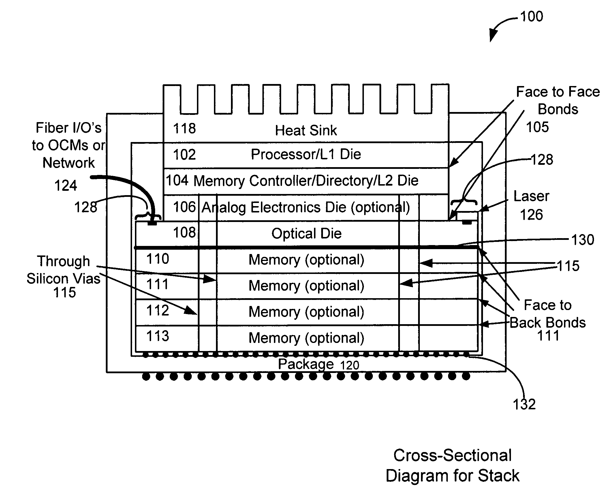
[0020]The present application discloses embodiments of a three-dimensional die stack architecture and packaging techniques. The embodiments disclosed herein may be used to advantageously replace wire-based electronic signaling for the global interconnect with an optical interconnect.

[0021]Advantageously, optical signaling does not suffer from the above-discussed problems with electrical signaling. This is because the energy required to send a bit of information with optics is not dependent on the length of the photonic waveguide for the distances of interest. Furthermore, the energy per bit using optical interconnect scales with VLSI technology and is orders of magnitude less than using an electrical interconnect. This, therefore, substantially mitigates the thermal problem. In addition, optical signaling does not suffer from a length-dependent coupled noise problem and hence the signal integrity problem is not an issue for optical signals.

[0022]Another problem overcome by some embo...


PUM


Abstract

Examples of a computer system packaged in a three-dimensional stack of dies are described. The package includes an electrical die and an optical die coupled to and stacked with the electrical die. The electrical die includes circuitry to process and communicate electrical signals, and the optical die includes structures to transport optical signals. The electrical die has a smaller area than the optical die so that the optical die includes an exposed mezzanine which is configured with optical input / output ports. Additionally, the packaging can be configured to provide structural support against insertion forces for external optical connections.

Description

BACKGROUNDCross Reference to Related Applications[0001]This patent application may contain subject matter related to the following patent applications, all of which are hereby incorporated by reference: (1) U.S. patent application Ser. No. 11 / 975,974, entitled “PHOTONIC INTERCONNECTS FOR COMPUTER SYSTEM DEVICES,” filed Oct. 23, 2007, now U.S. Pat. No. 7,532,785; and (2) U.S. patent application Ser. No. 11 / 975,963, entitled “THREE-DIMENSIONAL MEMORY MODULE ARCHITECTURES” filed Oct. 23, 2007, U.S. Patent Publication No. 2009 / 0103345.TECHNICAL FIELD[0002]The present application relates generally to processors and memory for computer systems.DESCRIPTION OF THE BACKGROUND ART[0003]The growth of future silicon based computer systems is fundamentally limited by the inter-related problems of signal integrity, wire-based global signaling, and thermal properties. As integrated circuit process technology progressively shrinks transistor sizes, the wires that interconnect the transistors are in...

Claims


Application Information

Patent Timeline
Patent Type & Authority Patents(United States)
IPC IPC(8): G02B6/12G11C5/06
CPCG02B6/43H01L2924/0002H01L2224/16225H01L2924/00
Inventor BINKERT, NATHANJOUPPI, NORMDAVIS, ALBEAUSOLEIL, RAYMOND
Owner HEWLETT-PACKARD ENTERPRISE DEV LP
Why Eureka
Try Eureka