Method for manufacturing optical modulator, optical modulator, and optical modulation system

a manufacturing method and technology of optical modulators, applied in the direction of liquid surface applicators, instruments, coatings, etc., can solve the problems of many constraints on material selection, difficult to respond to the demand for miniaturization and integration, and difficulty in reducing operating voltage and cost, so as to improve light utilization efficiency

Inactive Publication Date: 2010-03-02
ROHM CO LTD
View PDF9 Cites 2 Cited by
  • Summary
  • Abstract
  • Description
  • Claims
  • Application Information

AI Technical Summary

Benefits of technology

[0014]The present invention has been made in view of these circumstances, and a general purpose thereof is to provide a manufacturing method for a light modulation device that improves light utilization efficiency.
[0016]According to this embodiment, by planarizing the upper surface of the light modulating film, it is possible to manufacture the light modulation device, in which light scattering is prevented, and light utilization efficiency is improved.
[0017]The planarization may be carried out so that irregularities on the upper surface of light modulating film are less than or equal to 1 / 100 of the wavelength of light incident on the light modulation device. In these cases, it is possible to manufacture the light modulation device, in which the light scattering is preferably prevented and the light utilization efficiency is improved. For example, when a blue-violet laser with a wavelength of 400 nm is used, the irregularities are less than or equal to 4 nm.

Problems solved by technology

However, with the optical shutter using the bulk PLZT, it is difficult to respond to demand for miniaturization and integration, and to demand for reduction in operating voltage and lowering of costs.
Furthermore, since the bulk method includes processing at a high temperature of 1000° C. or more, after mixing metal-oxide that is raw material, when applied to a device formation process, many constraints on selection of material, device structure, and the like, are added.
However, the inventors of the present invention found that in cases in which the formed light modulating film is used as it is, the intensity of the reflected light decreases with respect to the intensity of incident light in the light modulation device, that is, that the utilization efficiency of the light cannot easily be raised.

Method used


Image

  • Method for manufacturing optical modulator, optical modulator, and optical modulation system
  • Method for manufacturing optical modulator, optical modulator, and optical modulation system
  • Method for manufacturing optical modulator, optical modulator, and optical modulation system

Examples


Embodiment Construction

[0036]The invention will now be described based on preferred embodiments which do not intend to limit the scope of the present invention but exemplify the invention. All of the features and the combinations thereof described in the embodiment are not necessarily essential to the invention.

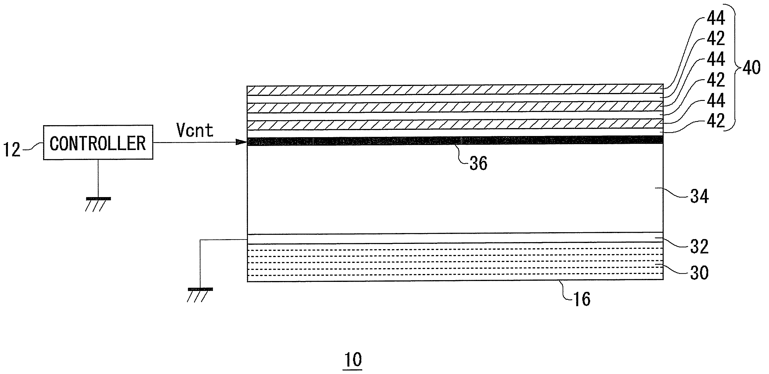
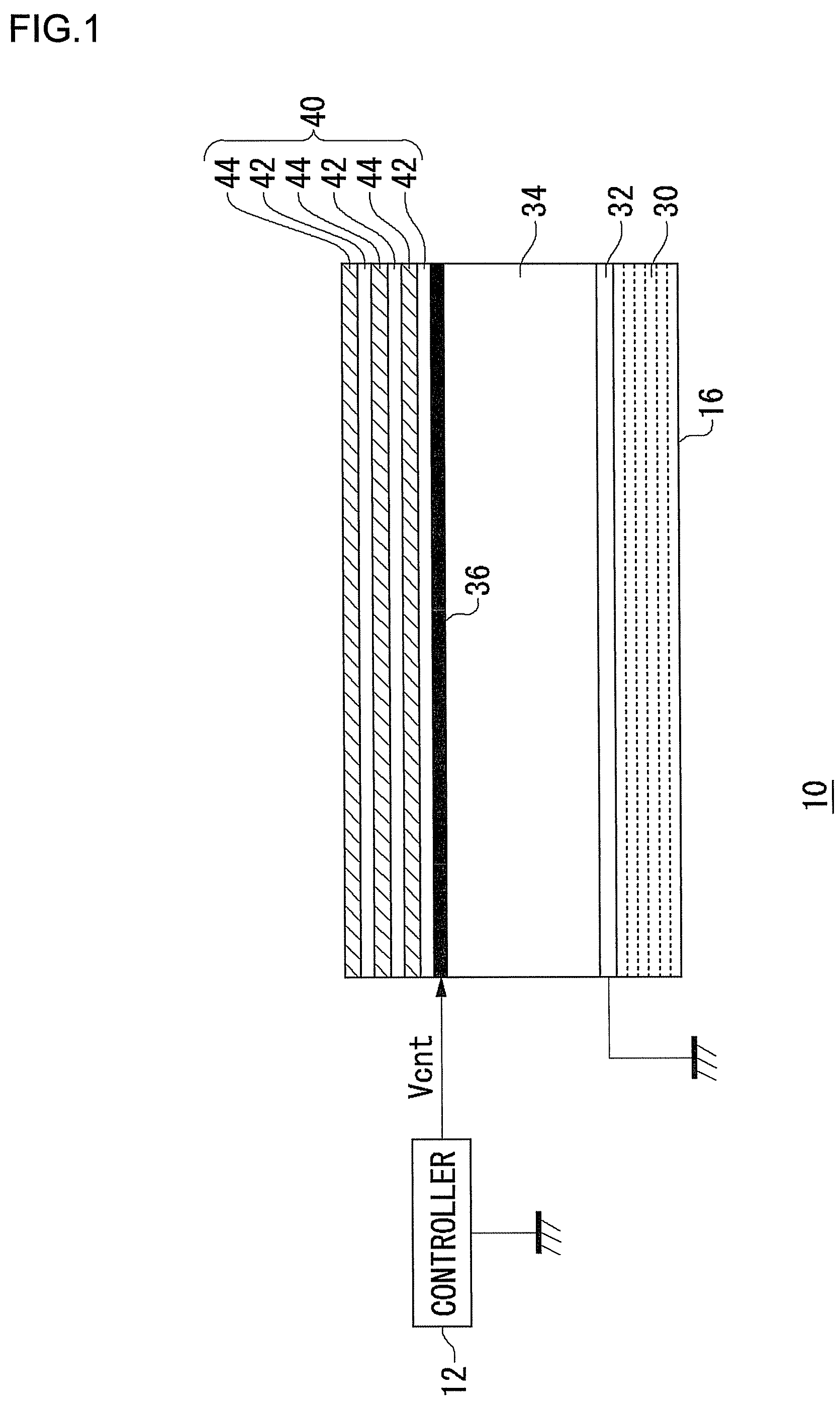
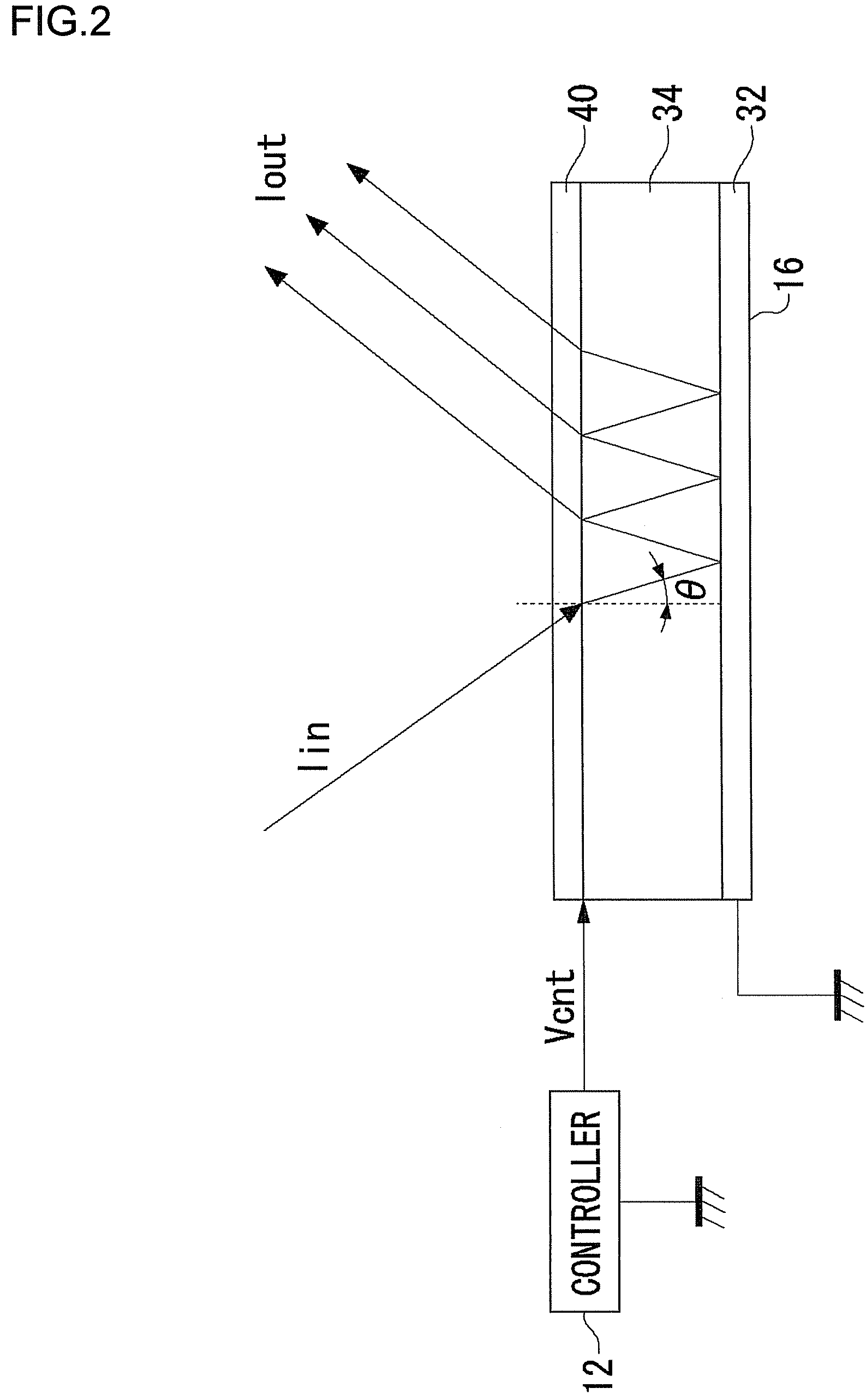
[0037]An outline of a light modulation device related to an embodiment will be explained. The light modulation device is one in which reflectance changes in accordance with voltage application from outside. The light modulation device has a Fabry-Perot type of resonator structure, and is provided with a light modulating film whose refractive index changes in accordance with an applied electrical field, and two reflective layers formed so as to sandwich the light modulating film. In a state in which a laser is incident on the light modulation device, when a control signal is provided, it is possible to change the reflectance of the light modulation device, and it is possible to control the intensity...


PUM

PropertyMeasurementUnit
refractive indexaaaaaaaaaa
temperatureaaaaaaaaaa
wavelengthaaaaaaaaaa

Abstract

A manufacturing method is provided for a light modulation device that improves utilization efficiency of light. After forming a first reflective layer using a metallic material such as Pt or the like, on a substrate, a light modulating film is formed using an electro-optic material in which refractive index changes in accordance with an applied electrical field. After that, planarization is carried out so that irregularities on an upper surface of the light modulating film are less than or equal to 1 / 100 of the wavelength of light incident on the light modulation device. A transparent electrode is then formed using ITO, ZnO, or the like, on the light modulating film, and a second reflective layer including a dielectric multilayer is formed.

Description

CROSS REFERENCE TO RELATED APPLICATIONS[0001]This is a U.S. national stage of application No. PCT / JP2006 / 307453, filed on 7 Apr. 2006. Priority under 35 U.S.C. §119(a) and 35 U.S.C. 365(b) is claimed from Japanese Application No. 2005-113763, filed 11 Apr. 2005, the disclosure of which is also incorporated herein by reference.BACKGROUND OF THE INVENTION[0002]1. Field of the Invention[0003]The present invention relates to a light modulation device that has a resonator structure.[0004]2. Description of the Related Art[0005]In recent years, as a recording method for large volumes, digital information recording systems that use the principle of holograms have become known (for example, Patent Document 1).[0006]As a material for a spatial light modulator of a hologram recording device, a material having electro-optical effects such as, for example, lead lanthanum zirconate titanate (referred to below as PLZT) or the like, can be used. PLZT is a transparent ceramic having a composition of...

Claims


Application Information

Patent Timeline
Patent Type & Authority Patents(United States)
IPC IPC(8): G02F1/03
CPCB82Y20/00G02F1/03G02F1/21G02F1/017G02F1/055G02F2001/213G02F1/213
Inventor FUJIMORI, YOSHIKAZU
Owner ROHM CO LTD
Why Eureka
Try Eureka