Method and structure for fabricating multiple tiled regions onto a plate using a controlled cleaving process

a technology of cleaving process and multi-layer substrate, which is applied in the direction of semiconductor/solid-state device manufacturing, basic electric elements, electric instruments, etc., can solve the problems of brittle materials, difficult to separate or cut extremely hard materials, and often difficult to achieve precision separation in the substrate for fine tools and assemblies, etc. , to achieve the effect of preventing the possibility of damage to the film or a remaining portion of the substrate, fewer implanting steps, and efficient processing

Inactive Publication Date: 2010-03-09
SILICON GENERAL CORPORATION
View PDF96 Cites 251 Cited by
  • Summary
  • Abstract
  • Description
  • Claims
  • Application Information

AI Technical Summary

Benefits of technology

[0013]Numerous benefits are achieved over pre-existing techniques using the present invention. In particular, the present invention uses controlled energy and selected conditions to preferentially cleave a plurality of thin films of material from a plurality of donor substrates, which includes multi-material sandwiched films. This cleaving process selectively removes the plurality of thin films of material from the substrates while preventing a possibility of damage to the film or a remaining portion of the substrate. Additionally, the present method and structures allows for more efficient processing using implantation of a plurality of donor substrates simultaneously according to a specific embodiment. Furthermore, the invention provides a method and structure to form large master donor substrates including a plurality of donor substrate regions using an economical approach and fewer implanting steps, as compared to conventional techniques. Depending upon the embodiment, one or more of these benefits may be achieved. These and other benefits may be described throughout the present specification and more particularly below.

Problems solved by technology

This technique, however, is often extremely “rough” and cannot generally be used for providing precision separations in the substrate for the manufacture of fine tools and assemblies.
Additionally, the saw operation often has difficulty separating or cutting extremely hard and or brittle materials, such as diamond or glass.
Additionally, the saw operation has difficulty in manufacturing larger substrates for flat panel displays and the like.
Amorphous silicon, however, suffers from a variety of known limitations.
Additionally, amorphous silicon may be difficult to use for high speed device applications due to its low relative carrier mobility.

Method used


Image

  • Method and structure for fabricating multiple tiled regions onto a plate using a controlled cleaving process
  • Method and structure for fabricating multiple tiled regions onto a plate using a controlled cleaving process
  • Method and structure for fabricating multiple tiled regions onto a plate using a controlled cleaving process

Examples


Embodiment Construction

[0018]According to the present invention, techniques related to the manufacture of substrates are provided. More particularly, the invention provides a technique including a method and a structure for forming multi-layered substrate structures, using a tiled approach, for the fabrication of devices, for example, on flat panel displays. But it will be recognized that the invention has a wider range of applicability; it can also be applied to other substrates for multi-layered integrated circuit devices, three-dimensional packaging of integrated semiconductor devices, photonic devices, piezoelectronic devices, microelectromechanical systems (“MEMS”), nano-technology structures, sensors, actuators, solar cells, biological and biomedical devices, and the like.

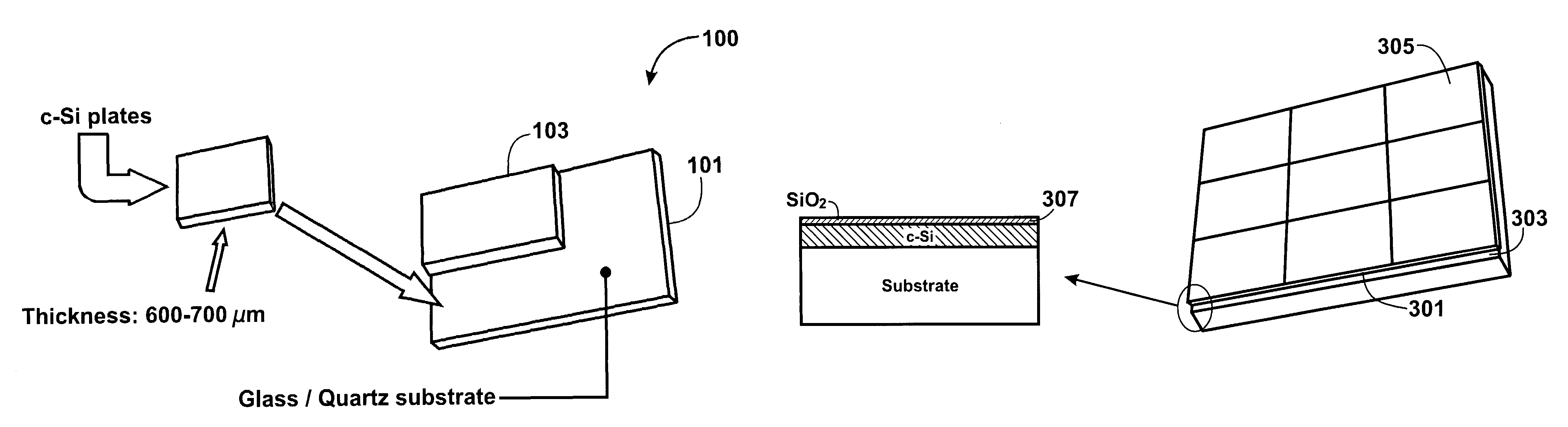
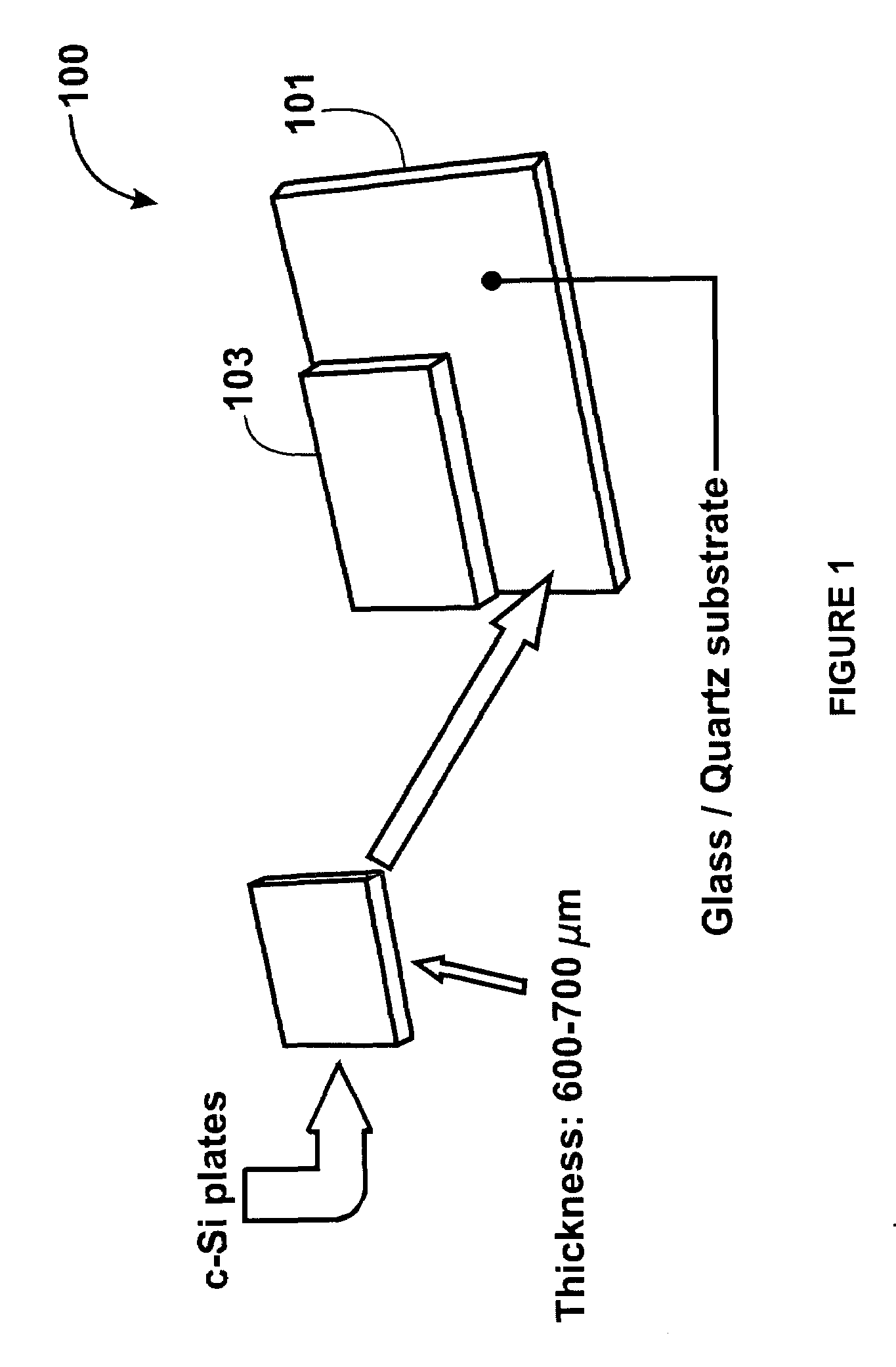
[0019]FIG. 1 is a simplified diagram illustrating a master tiled substrate member 100 according to an embodiment of the present invention. This diagram is merely an illustration that should not unduly limit the scope of the claims ...


PUM


Abstract

A reusable transfer substrate member for forming a tiled substrate structure. The member including a transfer substrate, which has a surface region. The surface region comprises a plurality of donor substrate regions. Each of the donor substrate regions is characterized by a donor substrate thickness and a donor substrate surface region. Each of the donor substrate regions is spatially disposed overlying the surface region of the transfer substrate. Each of the donor substrate regions has the donor substrate thickness without a definable cleave region.

Description

CROSS-REFERENCES TO RELATED APPLICATIONS[0001]NOT APPLICABLESTATEMENT AS TO RIGHTS TO INVENTIONS MADE UNDER FEDERALLY SPONSORED RESEARCH OR DEVELOPMENT[0002]NOT APPLICABLEREFERENCE TO A “SEQUENCE LISTING,” A TABLE, OR A COMPUTER PROGRAM LISTING APPENDIX SUBMITTED ON A COMPACT DISK[0003]NOT APPLICABLEBACKGROUND OF THE INVENTION[0004]The present invention relates to the manufacture of substrates. More particularly, the invention provides a technique including a method and a structure for forming multi-layered substrate structures, using a tiled approach, for the fabrication of devices, for example, on flat panel displays. But it will be recognized that the invention has a wider range of applicability; it can also be applied to other substrates for multi-layered integrated circuit devices, three-dimensional packaging of integrated semiconductor devices, photonic devices, piezoelectronic devices, microelectromechanical systems (“MEMS”), nano-technology structures, sensors, actuators, so...

Claims


Application Information

Patent Timeline
Patent Type & Authority Patents(United States)
IPC IPC(8): H01L21/30
CPCH01L21/26506H01L21/2658Y02E10/547
Inventor HENLEY, FRANCOIS J.
Owner SILICON GENERAL CORPORATION
Why Eureka
Try Eureka