Supercharge Your Innovation With Domain-Expert AI Agents!

Semiconductor memory device having a word line strap structure and associated configuration method

a memory device and word line technology, applied in the field of memory devices having word line strap structures, can solve the problems of difficult, if not impossible, to reduce the width of the metal line by using conventional metal processing technology, and the efficiency rate of reducing the layout area size is relatively low

Active Publication Date: 2010-03-09
SAMSUNG ELECTRONICS CO LTD
View PDF9 Cites 0 Cited by
  • Summary
  • Abstract
  • Description
  • Claims
  • Application Information

AI Technical Summary

Benefits of technology

The present invention is about a semiconductor memory device that has a word line strap structure. This structure reduces the length of the region where the conjunction portion of the memory cell array is located. The semiconductor memory device includes a memory cell array with sub-memory cell arrays, sense amplifying portions, contact and conjunction portions, and a main word line. The sub-memory cell arrays are arranged in a bit line direction and a word line direction perpendicular to the bit line direction. The sense amplifying portions are located between the sub-memory cell arrays in the bit line direction. The contact and conjunction portions are located between the sub-memory cell arrays in the word line direction. The main word line overlaps a word line of the sub-memory cell arrays in the word line direction. This structure reduces the size of the memory device and improves its performance.

Problems solved by technology

However, word line strap structures are rarely utilized in memory devices because it's difficult, if not impossible to reduce the width of the metal line by using conventional metal processing technology.
In addition, efficiency rates for reducing the layout area size are relatively low.
However, it is difficult to reduce the length C of conjunction portion CJ because the PMOS sense amplifier driver circuit, the NMOS sense amplifier driver circuit and the control circuit are all arranged in the conjunction portion CJ having the same width D as the width of the region where sense amplifying portion SA is arranged.
Thus, the efficiency for reducing the layout area size of the memory cell array is relatively low.
However, a drawback with this method is that the driving ability of the PMOS transistor driver and the NMOS transistor driver deteriorate.

Method used


Image

  • Semiconductor memory device having a word line strap structure and associated configuration method
  • Semiconductor memory device having a word line strap structure and associated configuration method
  • Semiconductor memory device having a word line strap structure and associated configuration method

Examples


Embodiment Construction

[0019]The present invention will now be described more fully hereinafter with reference to the accompanying drawings, in which preferred embodiments of the invention are shown. This invention, however, may be embodied in many different forms and should not be construed as limited to the embodiments set forth herein. Rather, these embodiments are provided so that this disclosure will be thorough and complete, and will fully convey the scope of the invention to those skilled in the art. In the drawings, like numbers refer to like elements throughout.

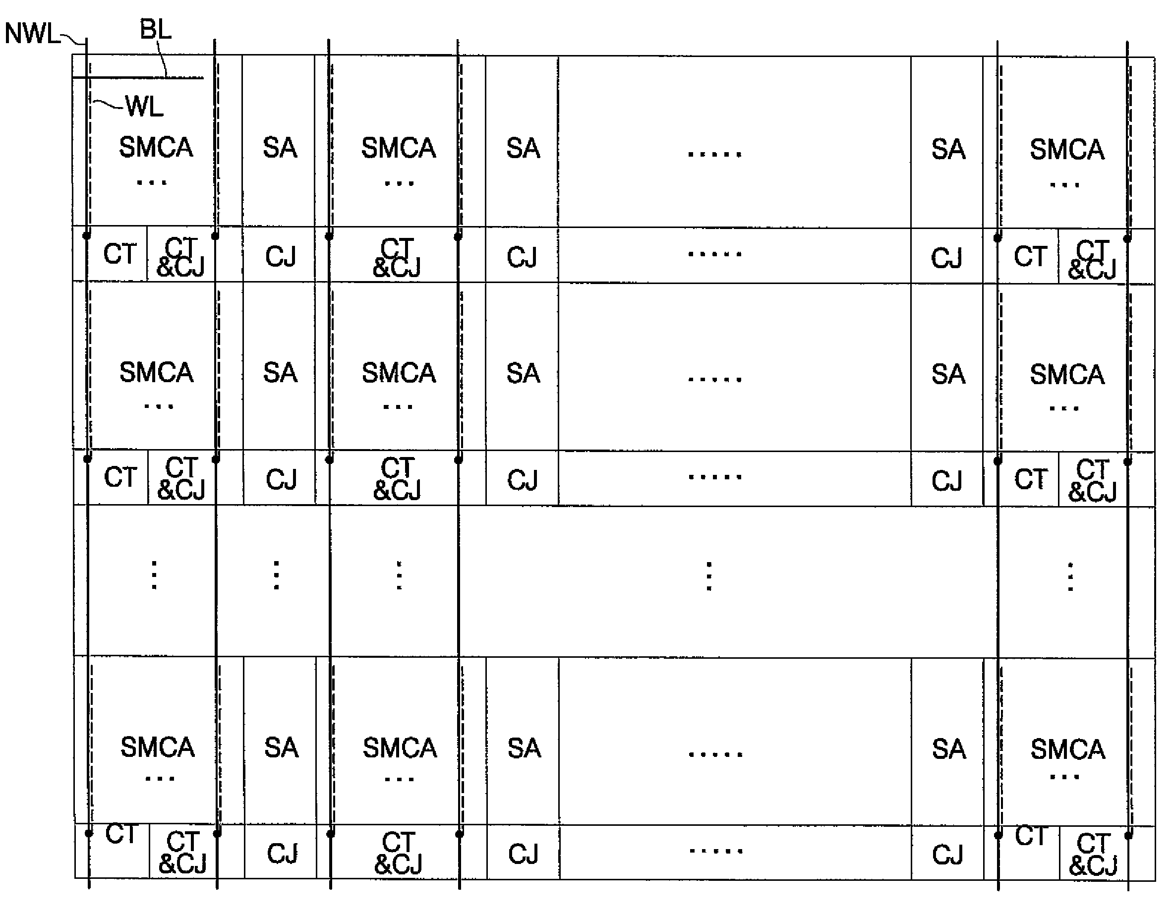
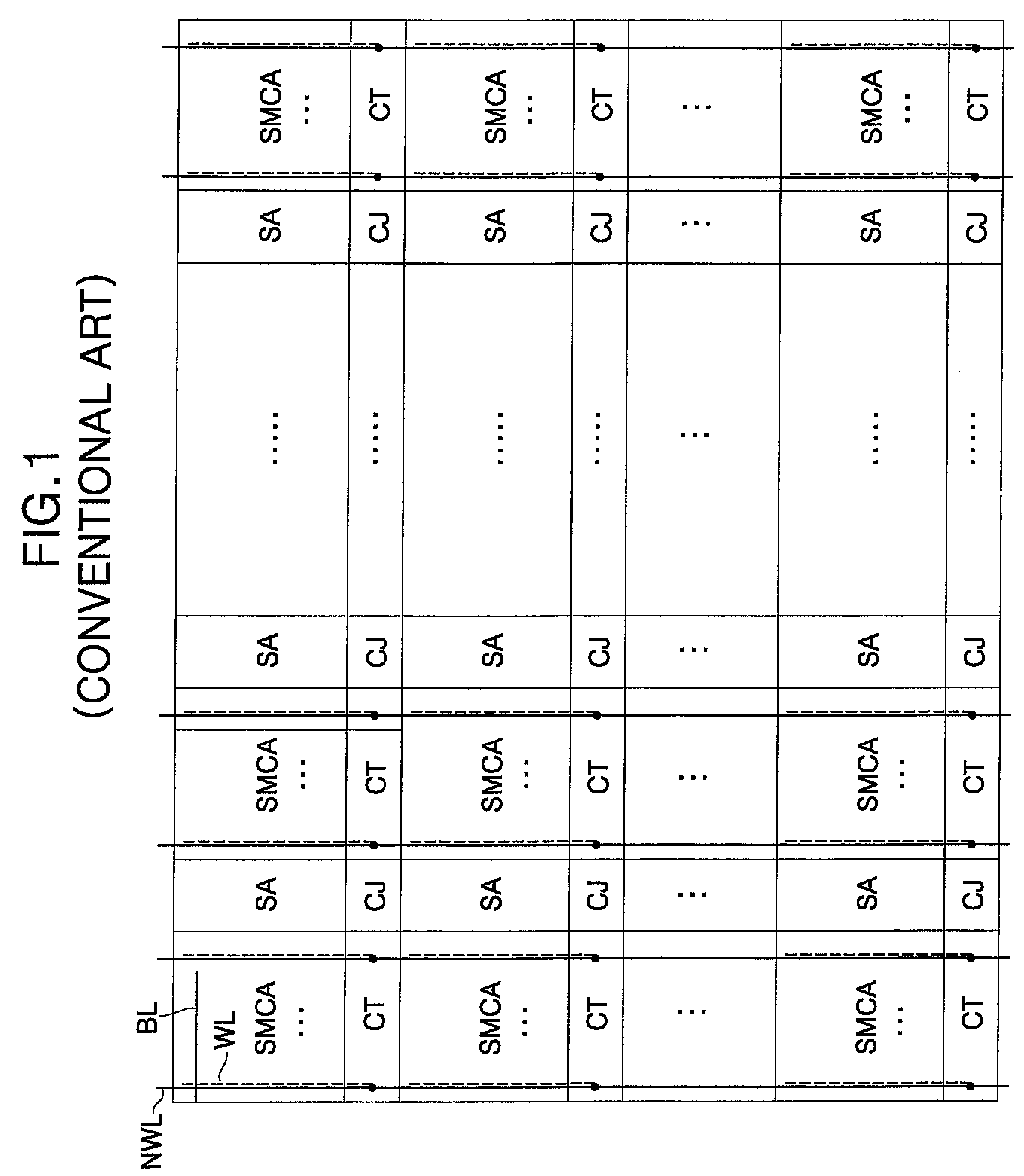
[0020]FIG. 3 shows a memory cell array of a semiconductor memory device having a word line strap structure according to an exemplary embodiment of the present invention. The memory cell array includes a sub-memory cell array SMCA and a sense amplifying portion SA alternately arranged in a bit line BL direction. A contact and conjunction portion CT & CJ are arranged between sub-memory cell arrays SMCA arranged in a word line WL direction. T...


PUM


Abstract

A semiconductor memory device having a memory cell array with sub-memory cell arrays arranged in a bit line direction and a word line direction which is perpendicular to the bit line direction. The memory cell arrays including a plurality of memory cells. The memory device further including sense amplifying portions arranged between the sub-memory cell arrays in the bit line direction, contact and conjunction portions arranged between the sub-memory cell arrays in the word line direction and conjunction portions arranged between the sense amplifiers in the word line direction. A main word line overlaps a word line between the sub-memory cell arrays arranged in the word line direction.

Description

CROSS-REFERENCE TO RELATED APPLICATION[0001]This U.S. non-provisional application claims priority under 35 U.S.C. §119 of Korean Patent Application No. 2006-90571 filed on Sep. 19, 2006, the entire contents of which are hereby incorporated by reference.BACKGROUND OF THE INVENTION[0002]1. Field of the Invention[0003]Embodiments of the invention relate to a semiconductor memory device. More particularly, embodiments of the invention relate to a semiconductor memory device having a word line strap structure.[0004]2. Discussion of Related Art[0005]A typical semiconductor memory device having a word line strap structure comprises a main word line made of metal which crosses over a memory cell array region. A word line made of poly crosses a sub-memory cell array unit of the memory cell array and overlaps the main word line. The main word line is connected to the word line of the memory cell array.[0006]Certain semiconductor memory devices include a word line strap structure which provide...

Claims


Application Information

Patent Timeline
Patent Type & Authority Patents(United States)
IPC IPC(8): G11C8/00
CPCG11C5/025G11C7/12G11C8/14G11C11/4094G11C7/18G11C11/4072G11C11/4091
Inventor KIM, JIN-YOUNG
Owner SAMSUNG ELECTRONICS CO LTD
Features
  • R&D
  • Intellectual Property
  • Life Sciences
  • Materials
  • Tech Scout
  • Unparalleled Data Quality
  • Higher Quality Content
  • 60% Fewer Hallucinations
Learn More