Unlock instant, AI-driven research and patent intelligence for your innovation.

Resistive memory architectures with multiple memory cells per access device

a memory cell and access device technology, applied in the field of resistive memory devices, can solve the problems of large power consumption, devices unsuitable for portable devices or as substitutes for frequently-accessed volatile memory devices

Active Publication Date: 2010-03-23
OVONYX MEMORY TECH LLC
View PDF11 Cites 17 Cited by
  • Summary
  • Abstract
  • Description
  • Claims
  • Application Information

AI Technical Summary

Benefits of technology

The patent text discusses the development of resistive memory devices, specifically phase change memory cells, which are non-volatile and have low power consumption. The text describes the various materials and methods used to create these memory cells, including the use of chalcogenides and GST materials. The technical effect of this invention is the creation of a more portable and energy-efficient memory device that can be used in portable devices or as a substitute for frequently-accessed volatile memory devices.

Problems solved by technology

Traditionally, however, non-volatile memory devices occupy a large amount of space and consume large quantities of power, making these devices unsuitable for use in portable devices or as substitutes for frequently-accessed volatile memory devices.
However, volatile memory devices require a continuous power supply in order to retain stored memory content.

Method used


Image

  • Resistive memory architectures with multiple memory cells per access device
  • Resistive memory architectures with multiple memory cells per access device
  • Resistive memory architectures with multiple memory cells per access device

Examples


Embodiment Construction

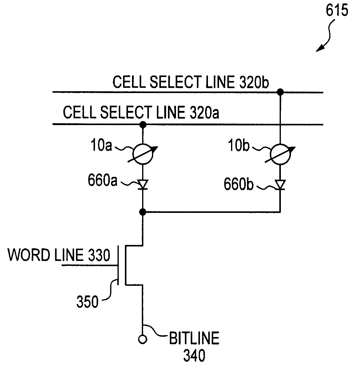
[0027]The large current requirements in variable resistance memory cells result in large access devices. When a variable resistance memory bit structure has a one-to-one pairing of memory cells to access devices, the memory bit structure has a large footprint. An example of the physical structure of a one-to-one memory cell to access device pairing is shown in FIG. 2C, which relates to portions of memory device 400 (FIG. 2B). In FIG. 2C, a cross-sectional view of the physical organization of two conventional memory bit structures 315c, 315e is depicted. The memory bit structures 315c, 315e share the same cell select line 320b and bit line 340b. Each memory bit structure 315c, 315e in FIG. 2C includes a memory cell 10a, 10b, respectively, that each include a top electrode 18, a bottom electrode 14, and a phase change region 16 positioned in between the electrodes 14, 18. The top electrode 18 of both memory cells 10a, 10b is connected to the cell select line 320b. The bottom electrode...


PUM


Abstract

A resistive memory structure, for example, phase change memory structure, includes one access device and two or more resistive memory cells. Each memory cell is coupled to a rectifying device to prevent parallel leak current from flowing through non-selected memory cells. In an array of resistive memory bit structures, resistive memory cells from different memory bit structures are stacked and share rectifying devices.

Description

FIELD OF THE INVENTION[0001]The embodiments of the invention relate generally to the field of semiconductor devices and, more particularly, to resistive memory devices, e.g., phase change memory devices.BACKGROUND OF THE INVENTION[0002]Microprocessor-accessible memory devices have traditionally been classified as either non-volatile or volatile memory devices. Non-volatile memory devices are capable of retaining stored information even when power to the memory device is turned off. Traditionally, however, non-volatile memory devices occupy a large amount of space and consume large quantities of power, making these devices unsuitable for use in portable devices or as substitutes for frequently-accessed volatile memory devices. On the other hand, volatile memory devices tend to provide greater storage capability and programming options than non-volatile memory devices. Volatile memory devices also generally consume less power than non-volatile devices. However, volatile memory devices...

Claims


Application Information

Patent Timeline
Patent Type & Authority Patents(United States)
IPC IPC(8): G11C11/00H10N80/00
CPCG11C13/0004H01L45/144G11C13/0026G11C13/003H01L27/2409H01L27/2436H01L27/2472H01L27/2481H01L45/06H01L45/1233G11C13/0023G11C2213/72G11C2213/74G11C2213/76G11C2213/78G11C2213/79H10B63/20H10B63/82H10B63/30H10B63/84H10N70/231H10N70/8828H10N70/826G11C16/02G11C16/00H10N70/841
Inventor LIU, JUNVIOLETTE, MIKE
Owner OVONYX MEMORY TECH LLC