Semiconductor device and manufacturing method thereof

a technology of semiconductor devices and semiconductor electrodes, applied in semiconductor devices, transistors, electrical devices, etc., can solve the problems of difficult to highly precisely maintain the distance lgf between the gate electrode b>, > and the field plate electrode , achieve improved yield, improved field plate electrode structure, and superior high frequency characteristics or performance

Inactive Publication Date: 2010-04-13
KK TOSHIBA
View PDF5 Cites 22 Cited by
  • Summary
  • Abstract
  • Description
  • Claims
  • Application Information

AI Technical Summary

Benefits of technology

[0017]The present invention was therefore conceived in consideration of the circumstances encountered in the related art mentioned above, and an object of the present invention is to provide a semiconductor device having an improved field plate electrode structure and having a superior high frequency characteristic or performance, and also provide a method for manufacturing the same with improved yield.
[0024]According to the present invention of the aspects mentioned above, a semiconductor device incorporating a field plate electrode and having high frequency characteristic can be obtained, and in addition, the method for manufacturing the same can be also provided with improved manufacturing yield.

Problems solved by technology

However, in the above conventional manufacturing method, since the gate electrode 55 and the field plate electrode 57 are formed in different steps, it has been difficult to highly precisely maintain the distance Lgf between the gate electrode 55 and the field plate electrode 57.

Method used


Image

  • Semiconductor device and manufacturing method thereof
  • Semiconductor device and manufacturing method thereof
  • Semiconductor device and manufacturing method thereof

Examples


embodiment 1

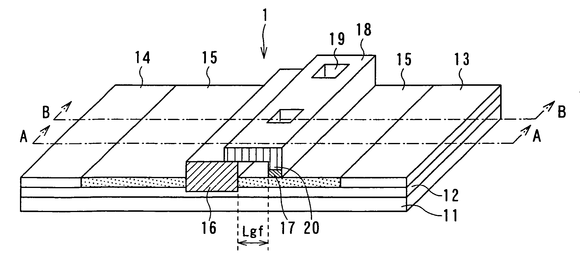
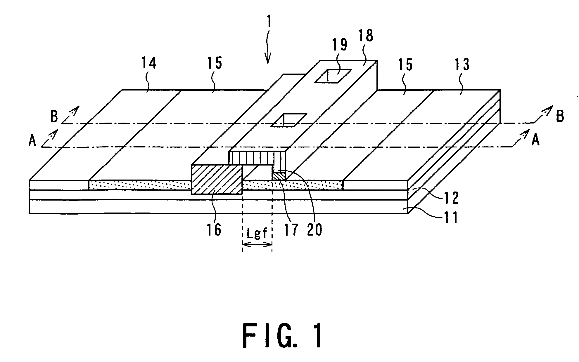
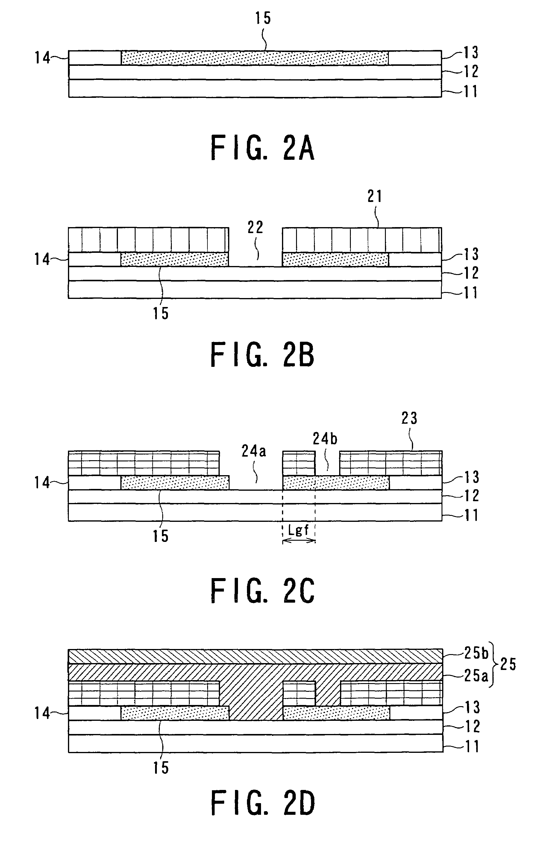
[0035]FIG. 1 is a schematic perspective view showing a semiconductor device according to one embodiment of the present invention. In a semiconductor device 1 shown in FIG. 1, a semiconductor substrate 11 is formed, for example, of GaAs, and on this semiconductor substrate 11, an channel layer 12 is formed. A drain electrode 13 and a source electrode 14 are formed on this channel layer 12 at portions apart from each other, and a gate electrode 16 is formed between the drain electrode 13 and the source electrode 14. In addition, a surface passivation film 15 is further formed on the channel layer 12 except for portions on which the drain electrode, 13, the source electrode 14 and the gate electrode 16 are formed.

[0036]Furthermore, a field plate electrode 17 is formed on the surface passivation film 15 between the gate electrode 16 and the drain electrode 13, at a predetermined distance Lgf from the gate electrode 16, the distance Lgf being a distance between inside surfaces thereof fa...


PUM


Abstract

A semiconductor device includes: an channel layer formed on a semiconductor substrate; a drain electrode and a source electrode both formed on the channel layer apart from each other; a surface passivation film formed on the channel layer so as to cover the channel layer except for the drain electrode and the source electrode; a gate electrode disposed between the drain electrode and the source electrode so as to penetrate the surface passivation film; a field plate electrode provided on the surface passivation film between the drain electrode and the gate electrode at a predetermined distance from the gate electrode; and a connecting plate having a bridge structure connecting the gate electrode to the field plate electrode. The bridge structure may be formed with at least one opening penetrating the connecting plate so as to face the surface passivation film with a predetermined space.

Description

CROSS REFERENCE TO RELATED APPLICATION[0001]This application is based upon and claims the benefit of priority from prior Japanese Patent Application No. 2005-067535 filed on Mar. 10, 2005, the entire contents of which are incorporated herein by reference.BACKGROUND OF THE INVENTION[0002]1. Field of the Invention[0003]The present invention relates to a semiconductor device having, particularly, an improved arrangement of a filed plate electrode (Fet), and a manufacturing method thereof.[0004]2. Related Art[0005]It has been well known that when a field plate electrode is provided for a semiconductor device, such as a field effect transistor, and is connected to the gate electrode thereof, the breakdown voltage of the semiconductor device can be improved.[0006]FIG. 7 is a schematic perspective view showing one example of a conventional semiconductor device having a field plate electrode, and a semiconductor device 50 shown in FIG. 7 is, for example, a GaAs field effect transistor. A ch...

Claims


Application Information

Patent Timeline
Patent Type & Authority Patents(United States)
IPC IPC(8): H01L29/74H01L21/4763
CPCH01L29/402H01L29/812H01L29/42316
Inventor MIYAO, AKIO
Owner KK TOSHIBA
Why Eureka
Try Eureka