Electron beam apparatus to collect side-view and/or plane-view image with in-lens sectional detector

a detector and electron beam technology, applied in the field of scanning electron microscopes, can solve the problems of difficult to achieve high resolution, poor aberration property of the sem layout, and the inability of the side-detector near the specimen surface to collect the side-view sem image to work

Active Publication Date: 2010-04-27
ASML NETHERLANDS BV
View PDF9 Cites 24 Cited by
  • Summary
  • Abstract
  • Description
  • Claims
  • Application Information

AI Technical Summary

Problems solved by technology

This conventional SEM layout has a poor aberration property, and it is difficult to achieve high resolution, especially for low landing energy SEM imaging.
Due to strong axial magnetic field and extraction electric field between the specimen surface and lens pole-piece of this compound lens, the layout of the side-detector near the specimen surface to collect the side-view SEM image cannot work anymore.

Method used


Image

  • Electron beam apparatus to collect side-view and/or plane-view image with in-lens sectional detector
  • Electron beam apparatus to collect side-view and/or plane-view image with in-lens sectional detector
  • Electron beam apparatus to collect side-view and/or plane-view image with in-lens sectional detector

Examples


Embodiment Construction

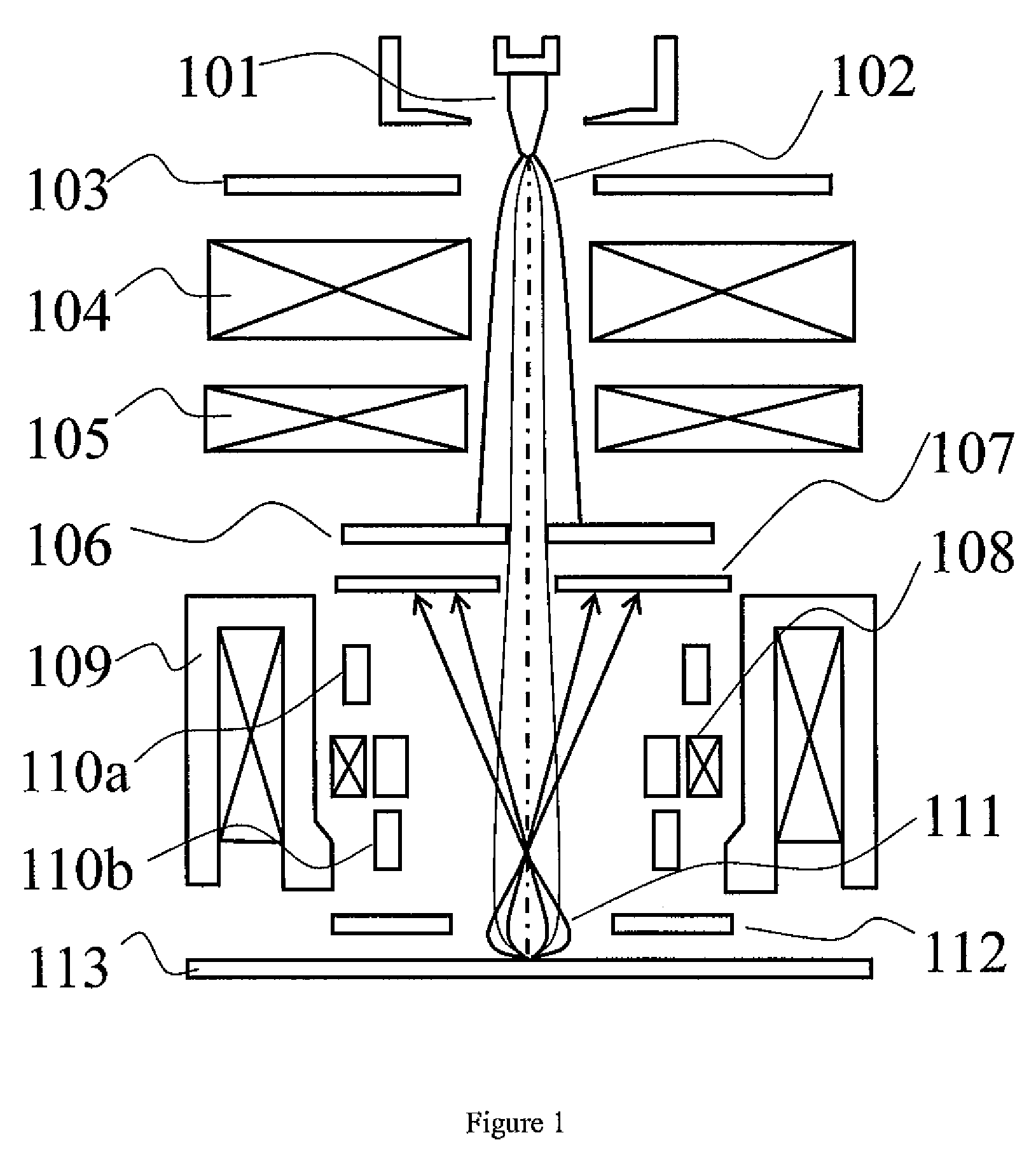
[0021]Reference will now be made in detail to specific embodiments of the invention. Examples of these embodiments are illustrated in accompanying drawings. While the invention will be described in conjunction with these specific embodiments, it will be understood that it is not intended to limit the invention to these embodiments. On the contrary, it is intended to cover alternatives, modifications, and equivalents as may be included within the spirit and scope of the invention as defined by the appended claims. In the following description, numerous specific details are set forth in order to provide a through understanding of the present invention. The present invention may be practiced without some or all of these specific details. In other instances, well known process operations have not been described in detail in order not to unnecessarily obscure the present invention.

[0022]The present invention may be implemented within any suitable measurement device that detects charged p...


PUM

PropertyMeasurementUnit
diameteraaaaaaaaaa
azimuth angleaaaaaaaaaa

Abstract

An electron beam apparatus and method are presented for collecting side-view and plane-view SEM imagery. The electron beam apparatus includes an electron source, some intermediate lenses if needed, an objective lens and an in-lens sectional detector. The electron source will provide an electron beam. The intermediate lenses focus the electron beam further. The objective lens is a combination of an immersion magnetic lens and a retarding electrostatic lens focuses the electron beam onto the specimen surface. The in-lens detector will be divided into two or more sections to collect secondary electrons emanating from the specimen with different azimuth and polar angle so that side-view SEM imagery can be obtained.

Description

CROSS-REFERENCE TO RELATED APPLICATIONS[0001]This application claims the benefit of priority to U.S. Provisional Application No. 60 / 819,057, filed Jul. 7, 2006, and entitled, “Electron Beam Apparatus To Collect Side-View and / or Plane-View Image With In-Lens Sectional Detector”, all of which is incorporated herein by reference.BACKGROUND OF THE INVENTION[0002]The present invention is related generally to scanning electron microscopes and more particularly to a system and method to collect the side-view and plane-view SEM image.DESCRIPTION OF THE RELATED ART[0003]A low-landing energy, high resolution SEM (scanning electron microscope) with the capability of capturing a side-view and plane-view image is a very important metrology tool to inspect and review defects in a semiconductor wafer. This SEM accelerates the new wafer processing technology ramp and improves the yield during mass production. For the conventional SEM with capability of collecting side-view SEM image of specimen, on...

Claims


Application Information

Patent Timeline
Patent Type & Authority Patents(United States)
IPC IPC(8): G01N23/00G21K7/00
CPCG01N23/225H01J37/244H01J37/28H01J2237/2449H01J2237/24465
Inventor TSENG, CHI-HUACHEN, ZHONG-WEILIU, XUEDONG
Owner ASML NETHERLANDS BV
Why Eureka
Try Eureka