Semiconductor package substrate

a technology of semiconductors and substrates, applied in semiconductor devices, semiconductor/solid-state device details, electrical devices, etc., can solve the problems of bump cracking and poor bonding between bumps, and achieve the effect of enhancing bonding strength

Active Publication Date: 2010-04-27
PHOENIX PRECISION TECH CORP
View PDF2 Cites 39 Cited by
  • Summary
  • Abstract
  • Description
  • Claims
  • Application Information

AI Technical Summary

Benefits of technology

[0010]In view of the drawbacks of the prior art, a primary objective of the present invention is to provide a semiconductor package substrate for enhancing the bonding strength between the semiconductor chips and the semiconductor package substrate after the reflow process.
[0011]Another objective of the present invention is to provide a semiconductor package substrate for increasing the layout density of the electrically connecting pads and providing a finer pitch.
[0015]Accordingly, the fabrication of the semiconductor package structure of the present invention involves forming first electrically connecting pads on the dielectric layer of the substrate body, using the first conductive vias in the dielectric layer to electrically connect with the first circuit layer, allowing the first electrically connecting pads to be completely exposed from the dielectric layer without having extending circuits, followed by a reflow process on the adhesive layer to allow the bumps of the semiconductor chip and the adhesive layer to fuse together and completely cover the first electrically connecting pads, so as to enhance the bonding strength between the semiconductor chip and the first electrically connecting pads, as well as to avoid incomplete coverage resulting in stress concentration. Moreover, since there is no circuits being disposed between the first electrically connecting pads, it is feasible to elevate the density of the first electrically connecting pads being disposed, thus is preferred for fine-pitch electrical connection.

Problems solved by technology

Hence, a circuit-extending portion of the electrically connecting pads 110 is susceptible to concentration of stress, thus leading to cracking of the bumps 22 and poor bonding between the bumps 22 and the electrically connecting pads 110.

Method used


Image

  • Semiconductor package substrate
  • Semiconductor package substrate
  • Semiconductor package substrate

Examples


first preferred embodiment

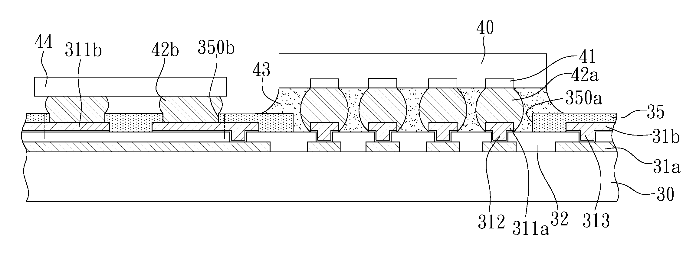
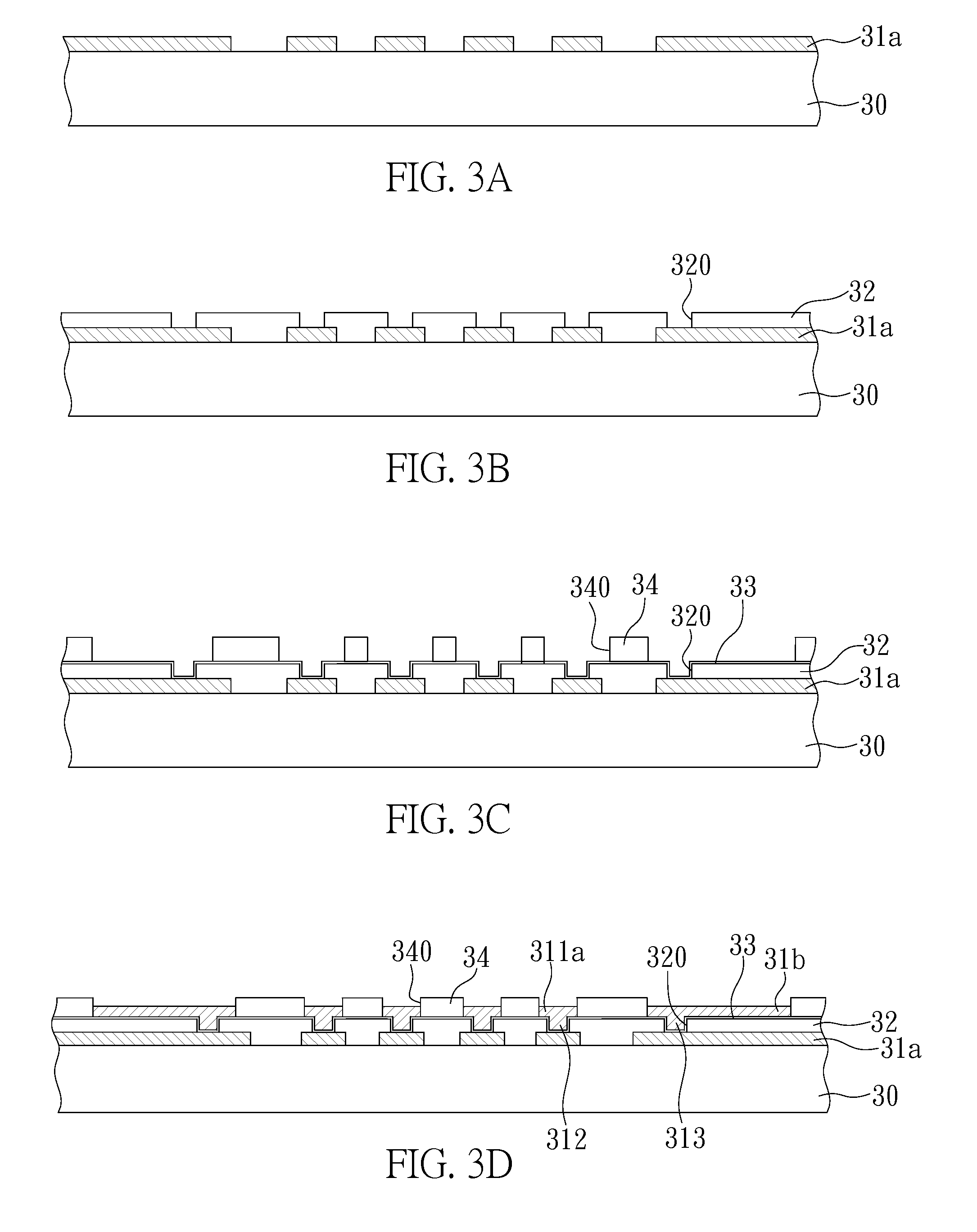
[0022]FIGS. 3A to 3G, and 4 are cross-sectional views of fabrication of a semiconductor package of the present invention.

[0023]Referring to FIG. 3A, a main body 30 with at least a surface having a first circuit layer 31a thereon is provided.

[0024]Referring to FIG. 3B, a dielectric layer 32 is formed on the main body 30 and the first circuit layer 31a, and a plurality of vias 320 are formed in the dielectric layer 32 for exposing a portion of the surface of the first circuit layer 31a.

[0025]Referring to FIG. 3C, a conductive layer 33 is formed on the dielectric layer 32, in the vias 320 and on a portion of the surface of the first circuit layer 31a using sputtering or chemical deposition such as electroless plating. The conductive layer 33 functions as a path whereby the electric current passes an electroplating metal material (described below) and is formed of metal, alloy, or several deposited layers of metal layers, such as copper, tin, nickel, chromium or copper-chromium alloy. ...


PUM


Abstract

A semiconductor package substrate includes a main body with a surface having a first circuit layer thereon and a dielectric layer covering the first circuit layer, with a plurality of vias on a portion of the first circuit layer; a plurality of first conductive vias disposed in the vias; a plurality of first electrically connecting pads on the first conductive vias and completely exposed on the dielectric layer having no extending circuits for a semiconductor chip to be mounted thereon, the first electrically connecting pad being electrically connected to the first circuit layer of the first conductive via; and an insulating protective layer disposed on the main body with an opening for completely exposing the first electrically connecting pads, whereby the circuit layout density is increased without disposing circuits between the electrically connecting pads.

Description

BACKGROUND OF THE INVENTION[0001]1. Technical Field[0002]The present invention relates to semiconductor package substrates, and more particularly, to first electrically connecting pads of a semiconductor package substrate for fine pitch application and enhanced bonding of semiconductor chips.[0003]2. Description of Related Art[0004]In flip-chip technology, electrode pads are formed on the IC semiconductor chip and an organic circuit board also has electrically connecting pads corresponding to the electrode pads in position. Solder structures or other conductive adhesive materials are formed between the electrode pads and the circuit boards for providing electrical and physical connections between the semiconductor chip and the circuit board. Related technology is disclosed in U.S. Pat. No. 6,809,262 (TW Patent No. 572361).[0005]Referring to FIGS. 1A and 1B, a circuit layer 11 is formed on at least one surface of a substrate main body 10. The circuit layer 11 comprises a plurality of...

Claims


Application Information

Patent Timeline
Patent Type & Authority Patents(United States)
IPC IPC(8): H01L23/498
CPCH01L21/563H01L23/49822H01L23/49894H01L2224/73203H01L2924/01078H01L2924/12044H01L2224/16225H01L2224/73204H01L2224/32225H01L2924/00H01L2224/05571H01L2224/05573H01L2924/00014H01L2224/05599
Inventor HU, WEN-HUNG
Owner PHOENIX PRECISION TECH CORP
Why Eureka
Try Eureka