
Semiconductor device with improved breakdown properties and manufacturing method thereof

a technology of semiconductors and breakdown properties, applied in the direction of semiconductor devices, basic electric elements, electrical equipment, etc., can solve the problems of inability to resist indefinite voltage levels, material eventually succumbing, electron flow, etc., and achieve good breakdown characteristics

Active Publication Date: 2010-05-04
AMI SEMICON BELGIUM
View PDF8 Cites 17 Cited by
  • Summary
  • Abstract
  • Description
  • Claims
  • Application Information

AI Technical Summary

Benefits of technology

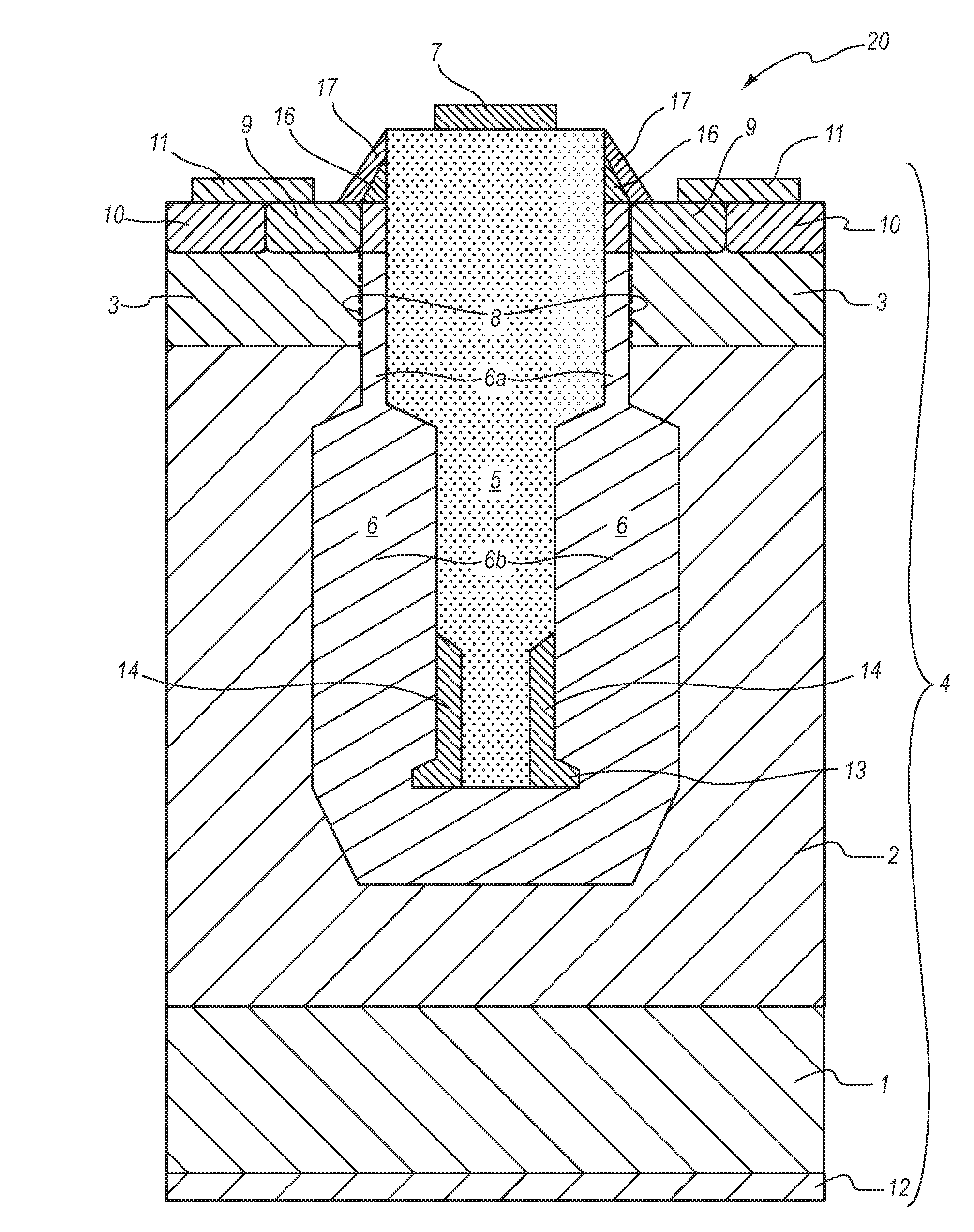
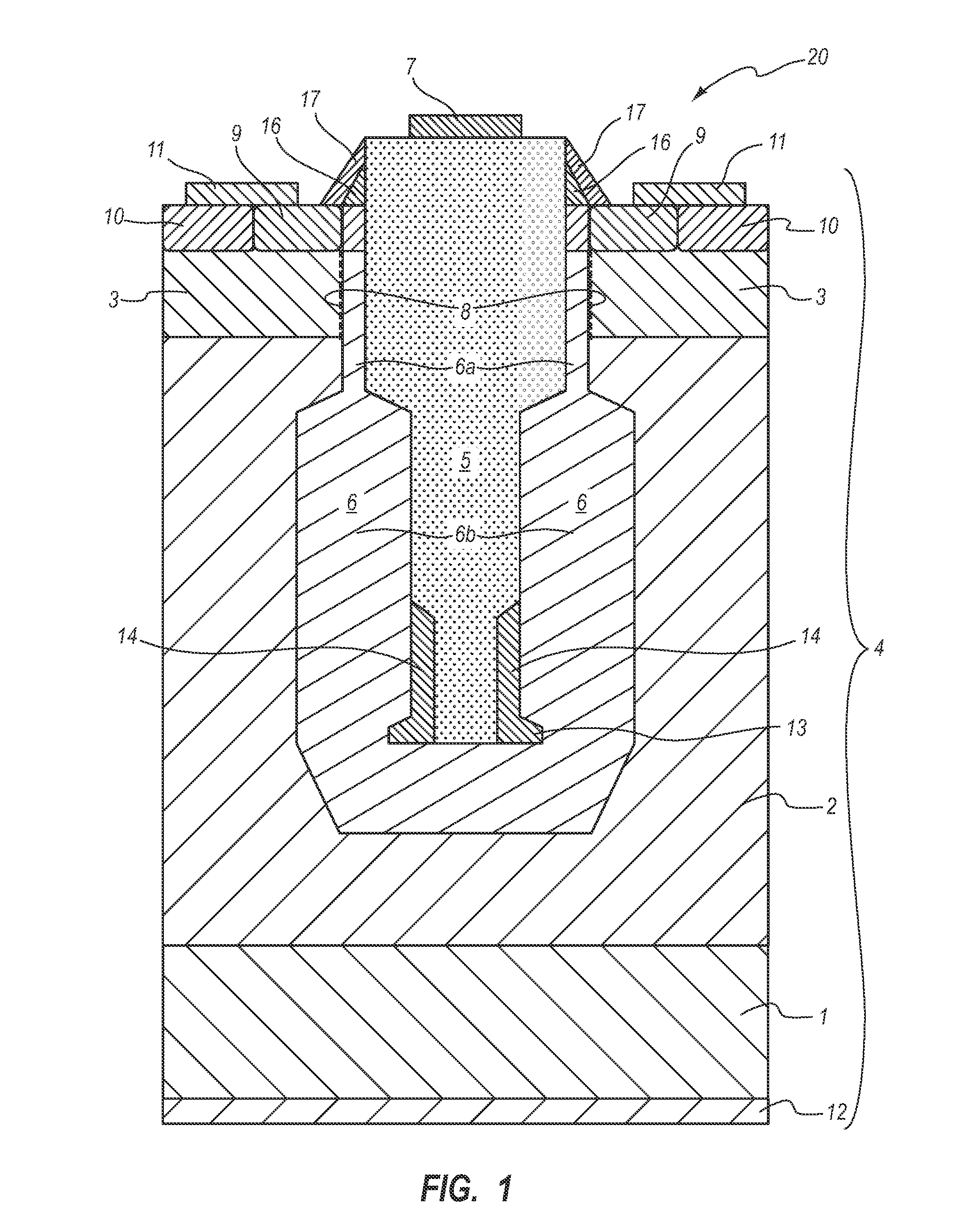
[0016]It is an object of the present invention to provide a semiconductor device with good breakdown characteristics and a method for manufacturing such a semiconductor device.
[0031]An advantage of the device according to embodiments of the invention is that it may comprise a higher breakdown voltage than the silicon limit and than devices comprising a thick grown dielectric, e.g. oxide, in a trench but not using spacers as in accordance with the present invention.
[0040]According to embodiments of the invention, the semiconductor device may furthermore comprise a floating dot region at the bottom of the trench in the second doped layer. The presence of a floating p-dot region further increases the breakdown voltage. The implant dopant dose in the floating dot region may be between 3·1012 cm−2 and 9·1012 cm−2.
[0041]According to embodiments of the invention, the semiconductor device may furthermore comprise an insulating etch stop on top of the first part of the first, e.g. grown, dielectric. The insulating etch stop may comprise a nitride spacer on top of the first, grown dielectric. According to other embodiments, the semiconductor device may furthermore comprise a protective oxide spacer on top of the nitride spacer for guaranteeing that the first, e.g. grown, dielectric layer is protected during further processing of the semiconductor device and that no short-circuit occurs between the control electrode, e.g. gate, and a main electrode, e.g. source electrode during this further processing.

Problems solved by technology

However, insulators cannot resist indefinite levels of voltage.
With enough voltage applied, any insulating material will eventually succumb to the electrical “pressure” and electron flow will occur, called insulator breakdown.
Also the maximum reverse bias voltage that can be applied to a p-n diode is limited by breakdown, breakdown being characterised by the rapid increase of the current under reverse bias.
This unstable electrical isolation behaviour may be associated with high electric fields across conventional isolation trenches and / or avalanche breakdown at the corners of conventional trench isolation structures.
In reality, this is impossible.
Doubling the voltage blocking capability typically leads to an increase in the on-state resistance by a factor of five—a physical law often referred to as the silicon limit for performance.
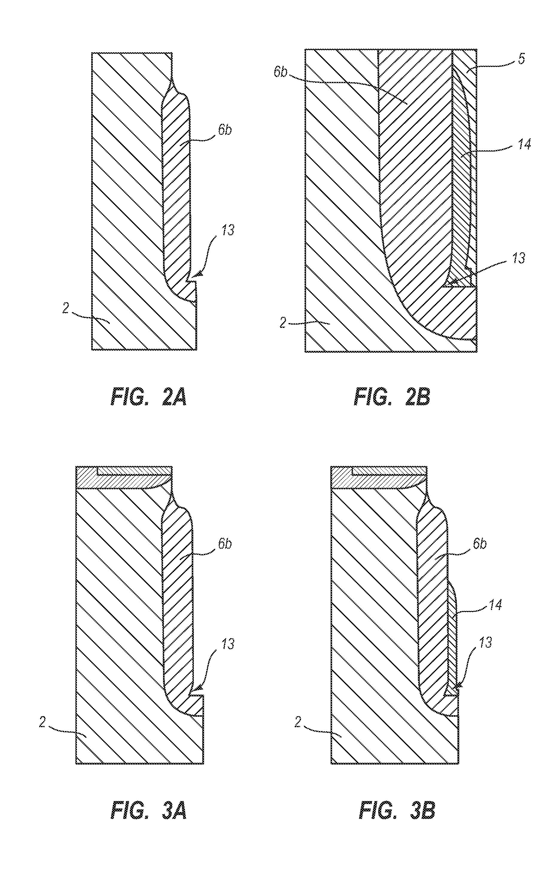
A disadvantage of the above-described devices is, that when growing the thick oxide in the trench, a notch can be formed at the bottom of the trench.
Because of this, a higher electric field will occur at this position which can result in premature breakdown of the device.

Method used


Image

  • Semiconductor device with improved breakdown properties and manufacturing method thereof
  • Semiconductor device with improved breakdown properties and manufacturing method thereof
  • Semiconductor device with improved breakdown properties and manufacturing method thereof

Examples


Embodiment Construction

[0076]The present invention will be described with respect to particular embodiments and with reference to certain drawings but the invention is not limited thereto but only by the claims. The drawings described are only schematic and are non-limiting. In the drawings, the size of some of the elements may be exaggerated and not drawn on scale for illustrative purposes. The dimensions and the relative dimensions do not correspond to actual reductions to practice of the invention.

[0077]Furthermore, the terms first, second, third and the like in the description and in the claims, are used for distinguishing between similar elements and not necessarily for describing a sequential or chronological order. It is to be understood that the terms so used are interchangeable under appropriate circumstances and that the embodiments of the invention described herein are capable of operation in other sequences than described or illustrated herein.

[0078]Moreover, the terms top, bottom, over, under...


PUM


Abstract

The present invention provides a semiconductor device (20) comprising a trench (5) formed in a semiconductor substrate formed of a stack (4) of layers (1,2,3), a layer (6) of a first, grown dielectric material covering sidewalls and bottom of the trench (5), the layer (6) including one or more notches (13) at the bottom of the trench (5) and one or more spacers (14) formed of a second, deposited dielectric material to fill the one or more notches (13) in the layer (6) formed of the first, grown dielectric material. The semiconductor device (20) according to the present invention shows improved breakdown voltage and on-resistance. The present invention furthermore provides a method for the manufacturing of such semiconductor devices (20).

Description

CROSS-REFERENCE TO RELATED APPLICATIONS[0001]This patent application claims the benefit of European patent application serial number 06015574.4, filed Jul. 26, 2006, which patent application is incorporated herein by reference in its entirety.TECHNICAL FIELD OF THE INVENTION[0002]The present invention relates to semiconductor devices with high breakdown voltage and a method for the manufacturing of such semiconductor devices.BACKGROUND OF THE INVENTION[0003]An important property of a semiconductor device is the breakdown voltage. There exists insulator breakdown and breakdown of p-n junctions.[0004]The atoms in insulating materials have very tightly-bound electrons, resisting free electron flow very well. However, insulators cannot resist indefinite levels of voltage. With enough voltage applied, any insulating material will eventually succumb to the electrical “pressure” and electron flow will occur, called insulator breakdown.[0005]Thickness of an insulating material plays a role ...

Claims


Application Information

Patent Timeline
Patent Type & Authority Patents(United States)
IPC IPC(8): H01L29/00
CPCH01L29/42368H01L29/513H01L29/7813H01L29/66719H01L29/66734H01L29/7809H01L29/0619H01L29/4916H01L29/495H01L29/517H01L29/665H01L29/6656H01L29/518
Inventor MOENS, PETERBAUWENS, FILIPBAELE, JORISTACK, MARNIX
Owner AMI SEMICON BELGIUM
Learn More