Solid-state imaging device and electronic device

a solid-state imaging and electronic device technology, applied in the direction of radio frequency controlled devices, instruments, television systems, etc., can solve the problems of difficult to prevent crosstalk between pixels, change in spectral characteristics, and inability to accurately obtain image data intended, so as to reduce crosstalk, improve image quality, and improve image quality

Inactive Publication Date: 2010-06-01
SONY SEMICON SOLUTIONS CORP
View PDF8 Cites 8 Cited by
  • Summary
  • Abstract
  • Description
  • Claims
  • Application Information

AI Technical Summary

Benefits of technology

[0018]A solid-state imaging device according to an embodiment of the present invention includes a light-shielding interlayer connecting material to connect layers of a multilayer structure to each other provided to at least part of a peripheral wiring portion. Therefore, the solid-state imaging device may improve image quality with a reduction in crosstalk.
[0019]An electronic device according to an embodiment of the present invention includes a solid-state imaging device that may improve image quality with a reduction in crosstalk. Therefore, the electronic device may use high-quality image data.

Problems solved by technology

Specifically, bright spots may be generated in an image that should be black, for example, so that image data intended may not be accurately obtained.
Therefore, it is difficult to prevent crosstalk from occurring between pixels in every solid-state imaging device having a photodiode, including any of CCD / CMOS solid-state imaging devices.
However, this method is known to have other problems such as a change in spectral characteristics.
However, this method is complicated because it may be necessary to carry out a separate process of forming the wall.

Method used


Image

  • Solid-state imaging device and electronic device
  • Solid-state imaging device and electronic device
  • Solid-state imaging device and electronic device

Examples


example

[0065]An example of the present embodiment will be described.

[0066]In the present example, there will be described results of examination based on simulation for the solid-state imaging device of the present embodiment.

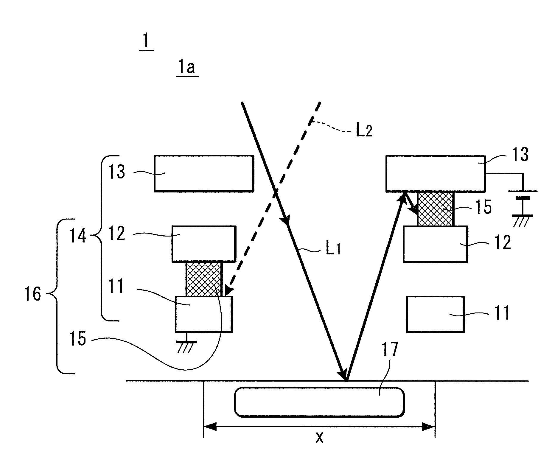
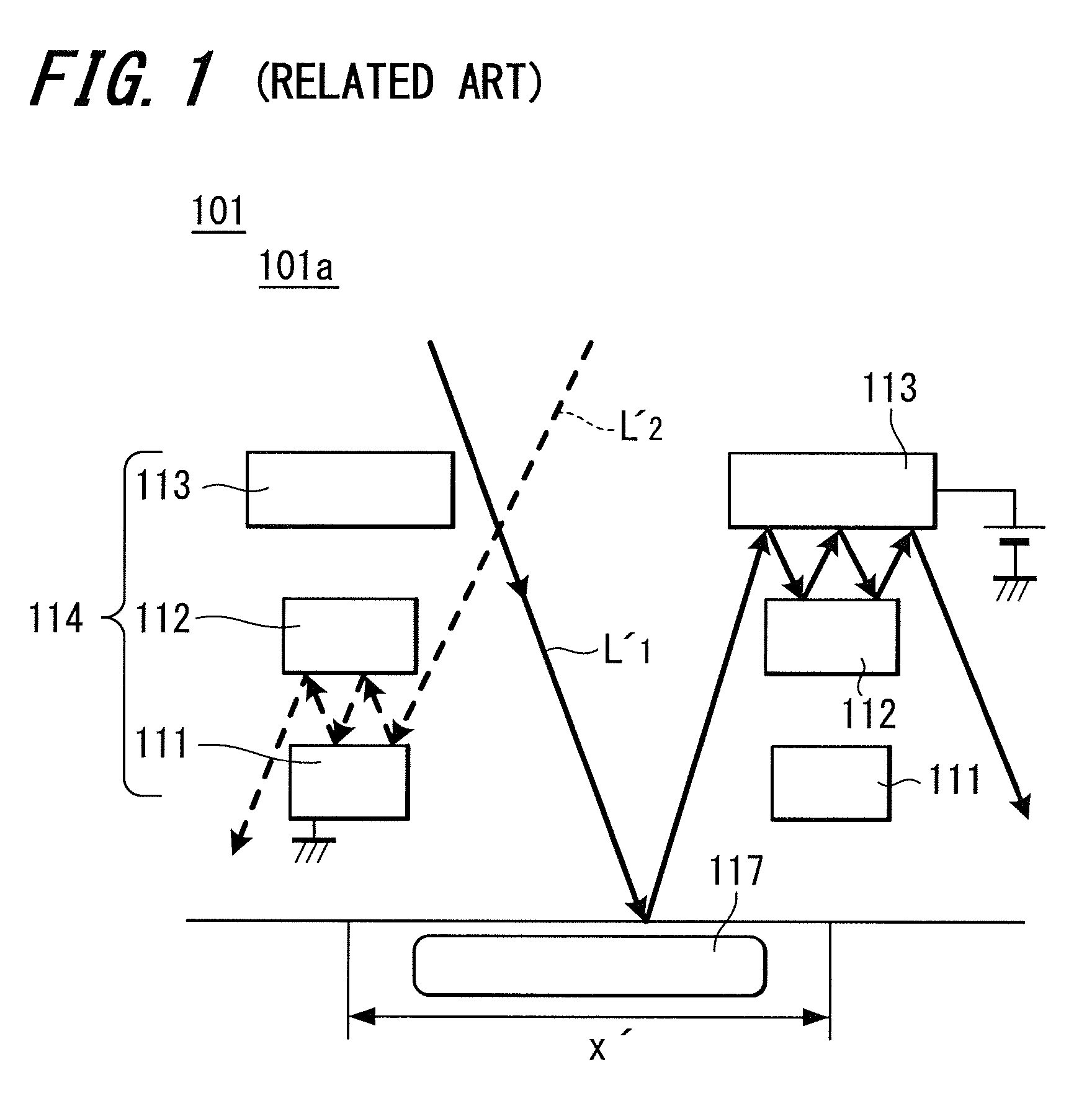
[0067]The solid-state imaging device according to the present embodiment is examined using a simulator. As a result, it may be confirmed that crosstalk caused by light reflected on a semiconductor substrate surface and the reflected light further reflected on a rear surface of an uppermost metal wiring is considerably reduced.

[0068]It may also be confirmed that, in a CMOS image sensor having a peripheral wiring portion with a wiring structure of three layers, for example, crosstalk caused by the following component is improved by 10% to 30%, although the value of improvement in such crosstalk varies according to a configuration of the multilayer wiring structure. Specifically, such component as reflected mainly by a rear surface of an uppermost metal wiring layer and ...


PUM

PropertyMeasurementUnit
lengthaaaaaaaaaa
shapeaaaaaaaaaa
voltageaaaaaaaaaa

Abstract

A solid-state imaging device including a number of pixels, each of which having a photoelectric converting portion, and which are arranged one-dimensionally or in a two-dimensional matrix. The solid-state imaging device includes a peripheral wiring portion with a multilayer structure provided around at least part of the photoelectric converting portion in each of the number of pixels and a light-shielding interlayer connecting material connecting layers of the multilayer structure to each other at least part of the peripheral wiring portion. The light-shielding interlayer connecting material is capable of reflecting or absorbing visible light.

Description

CROSS REFERENCES TO RELATED APPLICATIONS[0001]The present invention contains subject matter related to Japanese Patent Application JP 2006-290383 filed in the Japanese Patent Office on Oct. 25, 2006, the entire contents of which being incorporated herein by reference.BACKGROUND OF THE INVENTION[0002]1. Field of the Invention[0003]The present invention relates to a solid-state imaging device and an electronic device including the solid-state imaging device.[0004]2. Description of the Related Art[0005]Solid-state imaging devices are widely used as image input devices for various types of electronic devices such as digital still cameras, digital single-lens reflex cameras, digital video cameras, and portable terminals.[0006]A solid-state imaging device includes a number of pixels (picture cells) arranged in a two-dimensional matrix such as an array. The pixel has at least a photodiode as a photodetecting portion to convert light into electrons and a transfer portion. The transfer porti...

Claims


Application Information

Patent Timeline
Patent Type & Authority Patents(United States)
IPC IPC(8): H01L27/00G02F1/295H01L31/00H04N3/14H01J40/14H01L27/14H01L27/146H04N5/335H04N5/359H04N5/369H04N5/374H04N101/00
CPCH01L27/14623H01L27/14685H01L27/14636H01L27/1463H04N25/62
Inventor SATO, KIMIHIKOIIZUKA, TETSUYA
Owner SONY SEMICON SOLUTIONS CORP
Why Eureka
Try Eureka