Backlighting arrangement with semiconductor light sources arranged in light groups and lighting device

a technology of semiconductor light sources and backlighting arrangements, which is applied in the field of backlighting, can solve the problems of large space and power, large structural dimensions, and considerable loss of illuminating power, and achieve the effects of reducing good thermal conductivity, and avoiding undesirable inhomogeneous color effects

Inactive Publication Date: 2010-06-22
OSRAM OPTO SEMICON GMBH & CO OHG
View PDF23 Cites 43 Cited by
  • Summary
  • Abstract
  • Description
  • Claims
  • Application Information

AI Technical Summary

Benefits of technology

[0014]The objective underlying this invention is to bring about an improvement of color mixing in a backlighting arrangement or an illumination device in an economical manner.
[0035]An illumination device has a backlighting arrangement as described above and an optical element. Optimized color homogeneity can beneficially be produced with the illumination device pursuant to the invention.

Problems solved by technology

These radiate mostly white light, but require considerable space and power.
The increased separation, of course, causes undesirably large structural dimensions.
Diffusers between the light sources and the surfaces to be backlighted typically lead to considerable losses of illuminating power.
This impairs the overall efficiency of such backlighting and its feasibility.

Method used


Image

  • Backlighting arrangement with semiconductor light sources arranged in light groups and lighting device
  • Backlighting arrangement with semiconductor light sources arranged in light groups and lighting device
  • Backlighting arrangement with semiconductor light sources arranged in light groups and lighting device

Examples


Embodiment Construction

[0050]The illustrations of the backlighting arrangements in the figures are of schematic nature. The elements in the figures therefore do not correspond to reality, but are shown symbolically to be able to make the functioning of the arrangements more understandable.

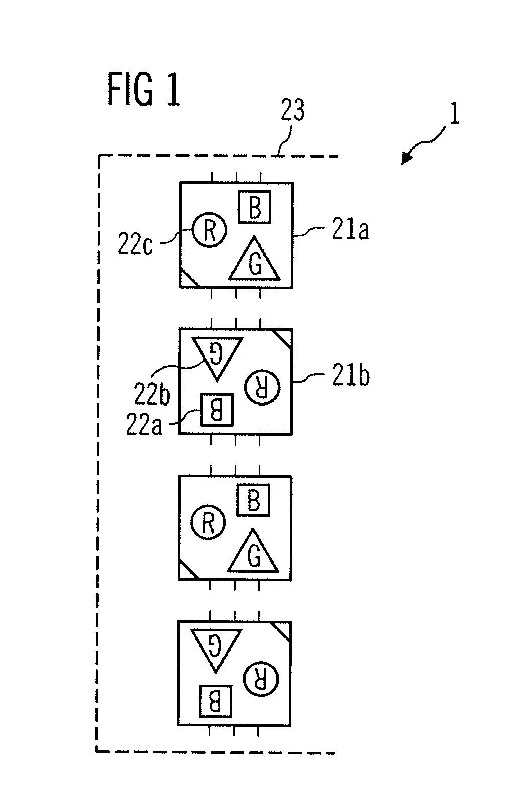
[0051]In the backlighting arrangement 1 of FIG. 1, little or no interfering color edge occurs. A red-emitting semiconductor component 22c, a green-emitting semiconductor component 22b, and a blue-emitting semiconductor component 22a alternately face the dashed line of the edge 23. This alternating color sequence comes into existence because each two adjacent illumination groups of the same construction 21a, 21b, each having a red-emitting semiconductor component 22c, a green-emitting semiconductor component 22b, and a blue-emitting semiconductor component 22a, are arranged turned by 180° with respect to one another relative to their principal directions of radiation.

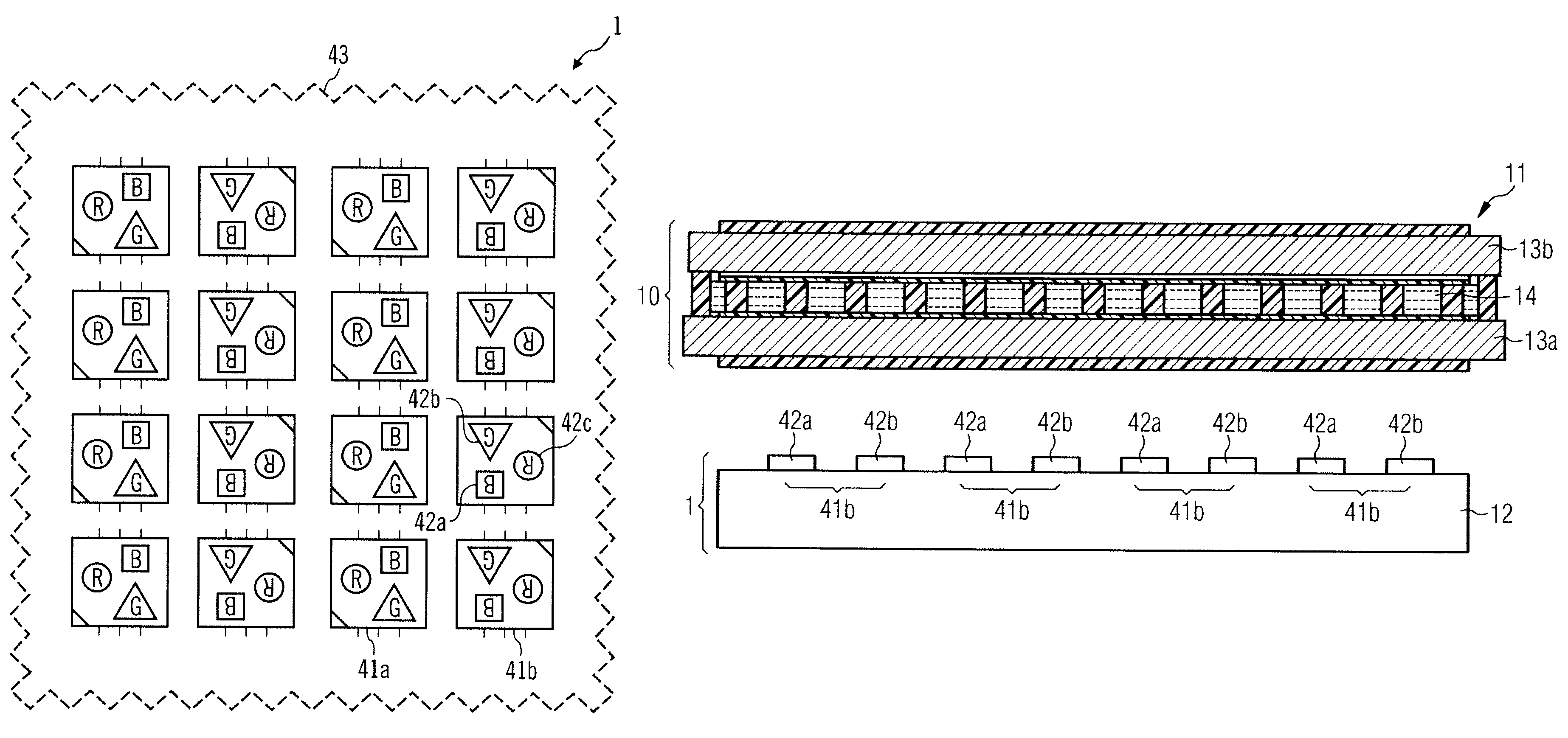
[0052]FIG. 2 shows a schematic representation of a seco...


PUM


Abstract

This invention relates to uniform backlighting of surfaces by semiconductor light sources. Various semiconductor light sources are combined into identical illumination groups. These identical illumination groups are arranged so that uniform backlighting of a surface is made possible. For homogeneous color mixing to be achieved, especially at edges, each illumination group in the arrangement has at least one adjacent illumination group in a different orientation.

Description

CROSS-REFERENCE TO RELATED APPLICATIONS[0001]This application is the National Stage of International Application No. PCT / DE2006 / 001550, filed Sep. 4, 2006, which claims priority to German Patent Application No. 10 2005 042 066.4, filed Sep. 3, 2005, the contents of which are incorporated herein by reference.FIELD OF INVENTION[0002]This invention relates to a backlighting arrangement with semiconductor light sources arranged in illumination groups. The invention also relates to an illumination device that has such a backlighting arrangement.BACKGROUND OF THE INVENTION[0003]This Patent Application claims the priority of German Patent Application 102005042066.4-54, the disclosure content of which is incorporated herewith by back reference.SUMMARY OF THE INVENTION[0004]Cold cathode fluorescent tubes have been used primarily up to now for the backlighting of surfaces such as LCDs (Liquid Crystal Displays). These radiate mostly white light, but require considerable space and power.[0005]T...

Claims


Application Information

Patent Timeline
Patent Type & Authority Patents(United States)
IPC IPC(8): G09F13/04F21K99/00H01L33/48
CPCG02F1/133603F21K9/00F21V5/007F21Y2101/02G02F2001/133613F21Y2105/003F21Y2105/12F21Y2105/10F21Y2115/10G02F1/133613G02F1/1335
Inventor HUTTNER, JOSEFOTT, HUBERTWANNINGER, MARIO
Owner OSRAM OPTO SEMICON GMBH & CO OHG
Why Eureka
Try Eureka