Test access control for plural processors of an integrated circuit

a technology of integrated circuits and access control, which is applied in the direction of error detection/correction, instruments, computing, etc., can solve the problems of insufficient consideration of the increase in the number of cpus to be debugged, increased cost, and insufficient time required for debugging, so as to facilitate debugging, reduce the number of microprocessors, and flexible addressing

Active Publication Date: 2010-06-22
RENESAS ELECTRONICS CORP
View PDF15 Cites 3 Cited by
  • Summary
  • Abstract
  • Description
  • Claims
  • Application Information

AI Technical Summary

Benefits of technology

[0008]An object of the present invention is to provide a technique for facilitating debugging in a semiconductor integrated circuit device including a plurality of microprocessors.
[0009]Another object of the present invention is to provide a technique capable of flexibly addressing an increase in the number of CPUs to be debugged in a semiconductor integrated circuit device which can be debugged by a single emulator.
[0019]To avoid undesirable increase in the number of external terminals of the semiconductor integrated circuit device including the plurality of microprocessors, the controller may include a fourth register capable of holding terminal control information for selectively coupling a signal output terminal from the plurality of processors to the common terminal.
[0022]The present invention can provide a technique capable of flexibly addressing an increase in the number of microprocessors to be debugged in a semiconductor integrated circuit device including a plurality of microprocessors. It can facilitate debugging in the semiconductor integrated circuit device including a plurality of microprocessors.

Problems solved by technology

In the first technique, when the number of processors mounted increases, it becomes necessary to add a debug terminal group and a debugging apparatus accordingly, so that the cost increases.
In the second technique, all of processors are debugged always via all of the TAP controllers, so that time required for debugging is long.
However, when the inventors of the present invention have examined the third technique, it was found out that the case where the number of CPUs to be debugged increases is not sufficiently considered.
For example, when the number of CPUs to be mounted increases due to a change in the specifications of a microcomputer or the like, the logic configuration of the selector is expected to be complicated, and it is difficult to flexibly address the increase in the number of CPUs.

Method used


Image

  • Test access control for plural processors of an integrated circuit
  • Test access control for plural processors of an integrated circuit
  • Test access control for plural processors of an integrated circuit

Examples


Embodiment Construction

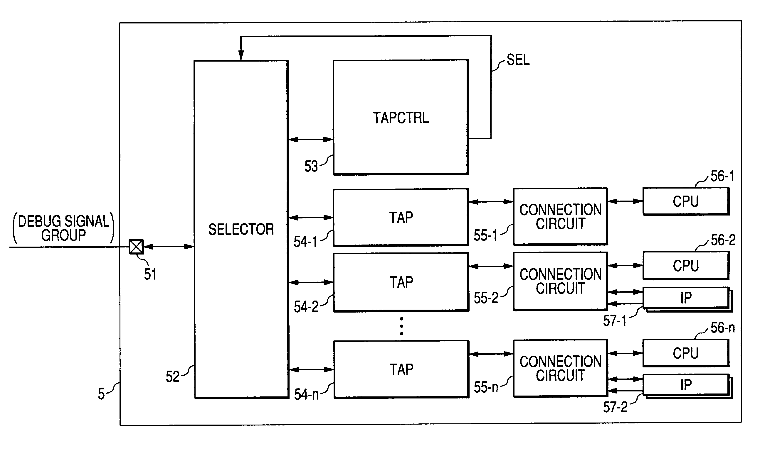
[0034]FIG. 5 shows a microcomputer as an example of a semiconductor integrated circuit device according to the present invention.

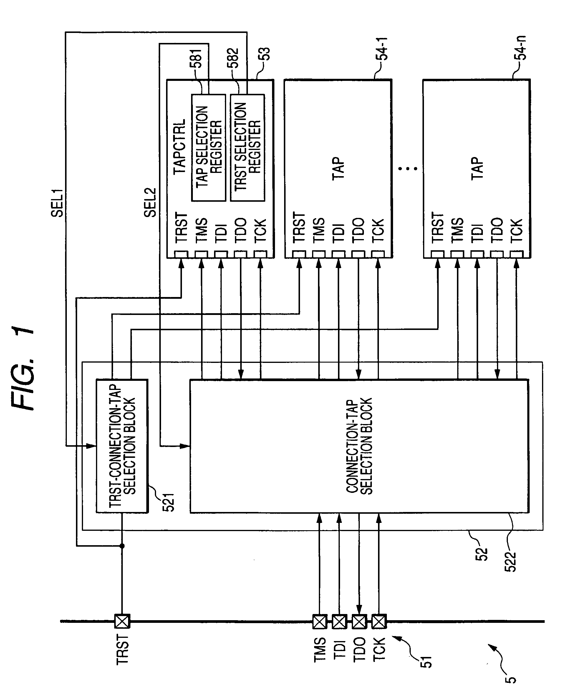
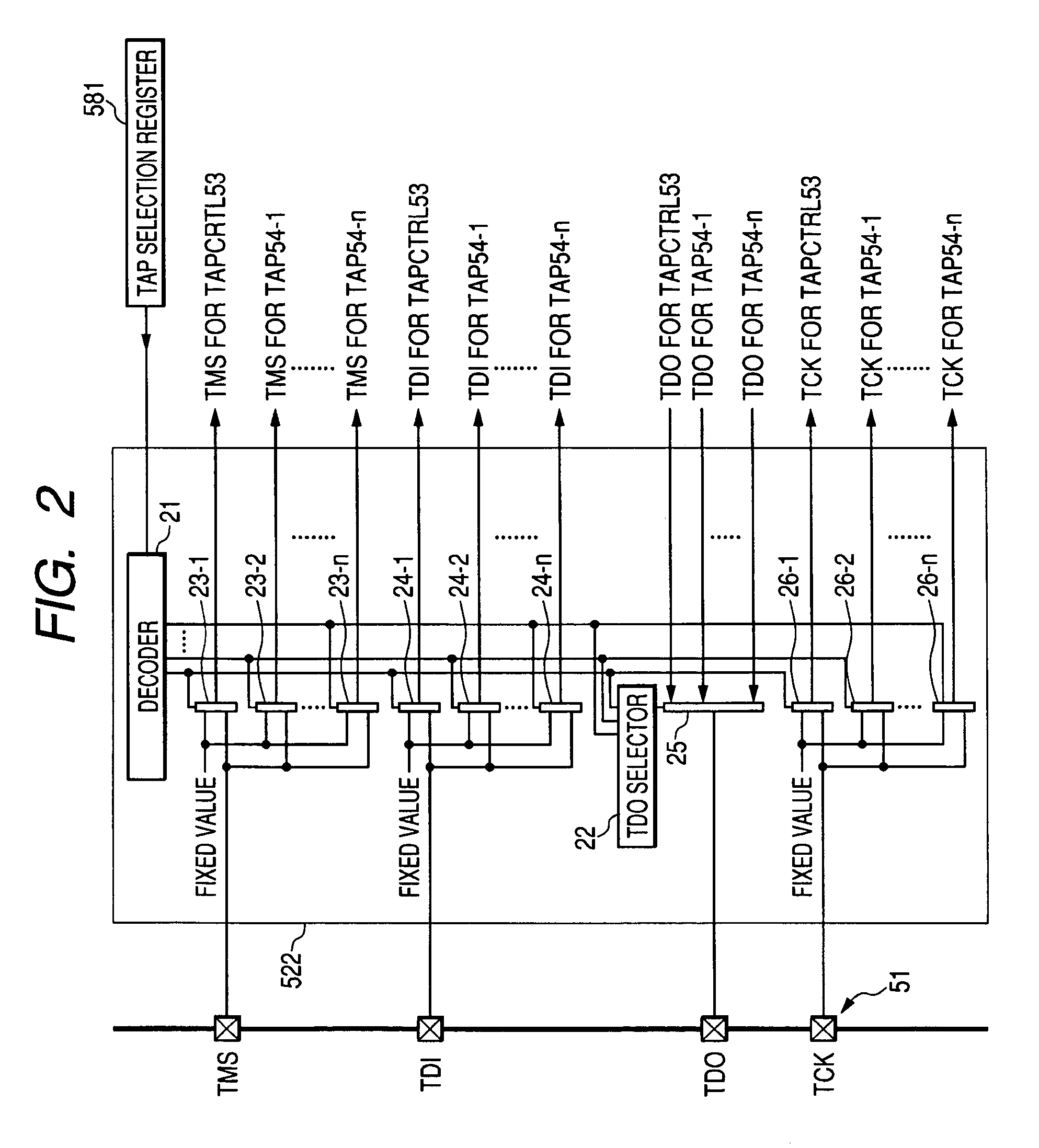
[0035]A microcomputer 5 shown in FIG. 5 includes, although not limited, a selector 52, a TAP controller (TAPCTRL) 53, (n+1) pieces of TAPs (Test Access Ports) 54-1, 54-2, . . . , and 54-n, connection circuits 55-1, 55-2, . . . , and 55-n, CPUs (Central Processing Units) 56-1, 56-2, . . . , and 56-n, and IP (Intellectual Property) modules 57-1 and 57-2 and, although not limited, is formed on a single semiconductor substrate such as a single-crystal silicon substrate by the known semiconductor integrated circuit manufacturing technique.

[0036]The selector 52 switches the TAPs 54-1, 54-2, and 54-n to which a JTAG (Joint Test Action Group) terminal group 51 as a test terminal group is connected. The switching is performed in accordance with a selection signal SEL obtained from the TAP controller 53. The CPUs 56-1, 56-2, . . . , and 56-n perform a predetermined ...


PUM


Abstract

The present invention is directed to facilitate debugging in a semiconductor integrated circuit device including a plurality of microprocessors. A semiconductor integrated circuit device includes: a plurality of processors; a plurality of debug interfaces enabling debugging of the corresponding processors; a plurality of common terminals shared by the plurality of debug interfaces; a selection circuit capable of selectively connecting the plurality of debug interfaces to the common terminals; and a controller capable of controlling selecting operation in the selection circuit in accordance with a predetermined instruction. A first selector capable of selectively connecting the plurality of debug interfaces to a TRST terminal in the terminal group conformed with the JTAG specifications, and a second selector capable of selectively connecting the plurality of debug interfaces to terminals other than the TRST terminal are provided. With the configuration, even in the case where the number of processors increases, the invention can flexibly address the increase.

Description

CROSS-REFERENCE TO RELATED APPLICATION[0001]The present application claims priority from Japanese patent application No. 2005-341958 filed on Nov. 28, 2005, the content of which is hereby incorporated by reference into this application.BACKGROUND OF THE INVENTION[0002]The present invention relates to a semiconductor integrated circuit device including a plurality of microprocessors and, more particularly, to a technique for facilitating debugging in the semiconductor integrated circuit device.[0003]A semiconductor integrated circuit device in which a plurality of microprocessors are formed on a single semiconductor substrate is a technique attracting attention in recent years.[0004]As a method of debugging a semiconductor integrated circuit device including a plurality of microprocessors, a first technique is known in which a group of debug terminals of the same number as that of mounted processors is provide for a semiconductor integrated circuit device, and debugging devices are c...

Claims


Application Information

Patent Timeline
Patent Type & Authority Patents(United States)
IPC IPC(8): G06F11/00
CPCG01R31/31705G01R31/318572
Inventor IKEDA, YURIAOTO, YOSHIKAZUMATSUSHIMA, JUNSASAKI, HIROYUKIUJII, TOMOYOSHISAEN, MAKOTO
Owner RENESAS ELECTRONICS CORP
Why Eureka
Try Eureka