Method for verifying mask pattern of semiconductor device

a semiconductor device and mask pattern technology, applied in the field of mask pattern verification of semiconductor devices, can solve the problems of difficult to detect defects on the actual wafer, different parts of the pattern between the actual wafer and the modified layout are detected as defects,

Active Publication Date: 2010-07-06
SK HYNIX INC
View PDF12 Cites 37 Cited by
  • Summary
  • Abstract
  • Description
  • Claims
  • Application Information

AI Technical Summary

Problems solved by technology

With the increase in integration degree of semiconductor devices, patterns required in semiconductor devices shrink in size gradually, which leads to pattern defects, e.g., a pattern bridge or a pinch fail, on an actual wafer due to limitations in a manufacturing process of semiconductor devices.
Once the original layout is modified, different parts between patterns on the actual wafer and a modified layout are detected as defects in the verification of pattern defects.
Therefore, it is difficult to detect defects occurring on the actual wafer, e.g., pattern bridges or pinch fails.

Method used


Image

  • Method for verifying mask pattern of semiconductor device
  • Method for verifying mask pattern of semiconductor device
  • Method for verifying mask pattern of semiconductor device

Examples


Embodiment Construction

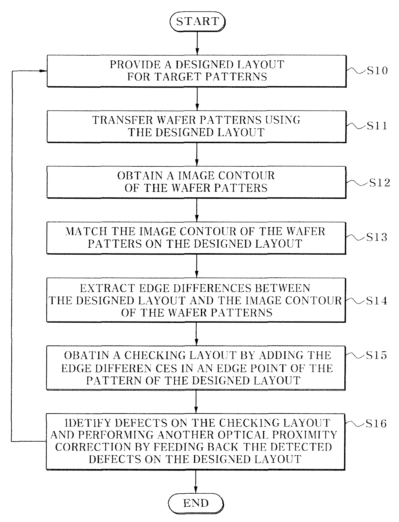
[0008]Hereinafter, a method for verifying a pattern of a semiconductor device in accordance with the preferred embodiment of the invention will be described in detail with reference to the accompanying drawings.

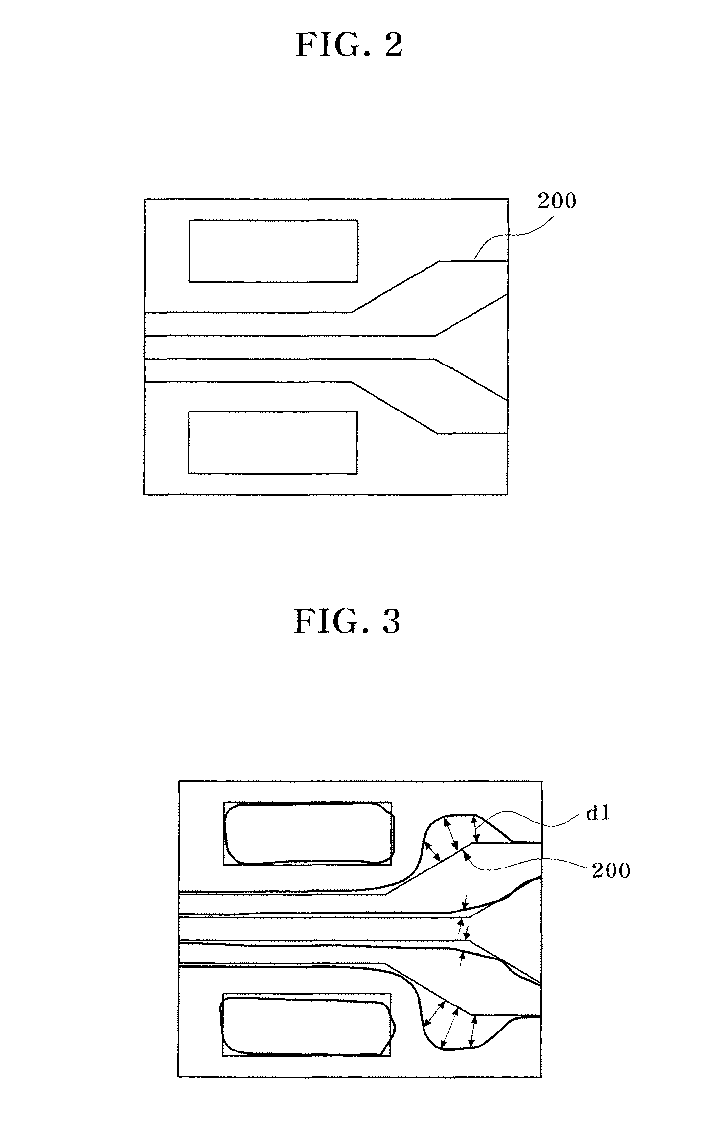
[0009]Referring to FIG. 1, a designed layout 200 is provided for target patterns, as illustrated in FIG. 2 (S10). In detail, a designer designs patterns using patterns to be realized on a wafer and data containing information. The layout 200 is designed in a layout editor such that it has the same shape as the wafer patterns which will be formed on an actual wafer. The layout 200 may be an original layout that a designer designs for the first time or an optical proximity corrected layout (OPC layout) for suppressing optical proximity effect on the original layout.

[0010]Wafer patterns is transferred on the actual wafer using the designed layout 200(S11). Specifically, a photomask having the same pattern configuration as the designed layout 200 for the target patterns is fabric...


PUM


Abstract

Provided is a method for verifying a pattern of a semiconductor device. In the method, a designed layout of target patterns is provided, and transferring the designed layout on a wafer to form wafer patterns. Wafer patterns image contour is obtain. The image contour for wafer patterns on the designed layout are matched, After edge differences between the designed layout and the wafer patterns image contour are extracted, a checking layout for detecting wafer pattern defects is obtain by adding the edge differences on the designed layout. Defects on the checking layout is identified to verify the patterns in view of processes before fabrication of a photomask.

Description

CROSS-REFERENCE TO RELATED APPLICATIONS[0001]This patent claims priority to Korean patent application number 10-2007-0063926, filed on Jun. 27, 2007, the disclosure of which is incorporated by reference in its entirety.BACKGROUND OF THE INVENTION[0002]This patent relates to a method for fabricating a semiconductor device, and more particularly, to a method for verifying a pattern of a semiconductor device.[0003]With the increase in integration degree of semiconductor devices, patterns required in semiconductor devices shrink in size gradually, which leads to pattern defects, e.g., a pattern bridge or a pinch fail, on an actual wafer due to limitations in a manufacturing process of semiconductor devices. Accordingly, before the verification of designed target patterns and the preparation of a mask, weak or defective parts in view of processes are detected in advance and the detection results are then reflected in a design layout.[0004]One of a conventional method for verifying patter...

Claims


Application Information

Patent Timeline
Patent Type & Authority Patents(United States)
IPC IPC(8): G06F17/50G06F9/45
CPCG06F17/5081G06F30/398G03F7/70433H01L21/0274
Inventor YANG, HYUN JO
Owner SK HYNIX INC
Why Eureka
Try Eureka