
Eureka
For R&D, Eureka makes reading and utilizing patents & technical documents easy.
Eureka AIR
Designed for self-driven R&D workflows. Generate viable solutions, solve complex R&D challenges, empower your innovation with AI.

Eureka Materials
Designed for material experts only. Revolutionize your material R&D, from search, analyze, to developing new materials.

TechResearch
Generate reliable direction feasibility study reports for your R&D in just a few steps.

TechSeek
Discover and master advanced knowledge NOW. Basics, ideas, possibilities, all at once.

TechMind
As an expert in R&D Theories, TechMind can generates customized viable solutions instantly.

TechRisk
Analyze your overall solution with one click, know your potential R&D risks in advance.

TechMonitor
Get weekly tech updates, stay abreast of the latest tech innovations and key insights.
Apparatus for cleaning edge of substrate and method for using the same
- Summary
- Abstract
- Description
- Claims
- Application Information
AI Technical Summary
Benefits of technology
Problems solved by technology
Method used
Image

Examples
Embodiment Construction
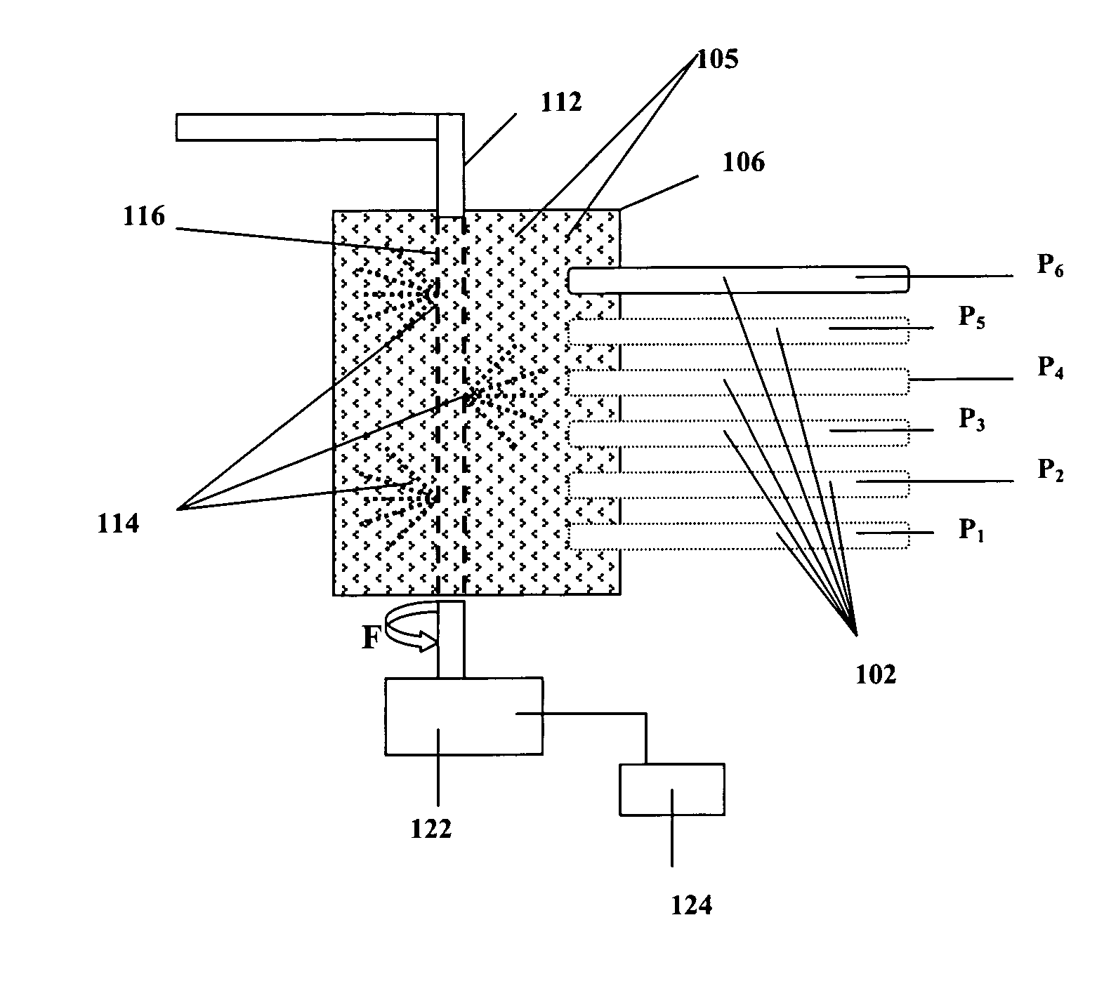
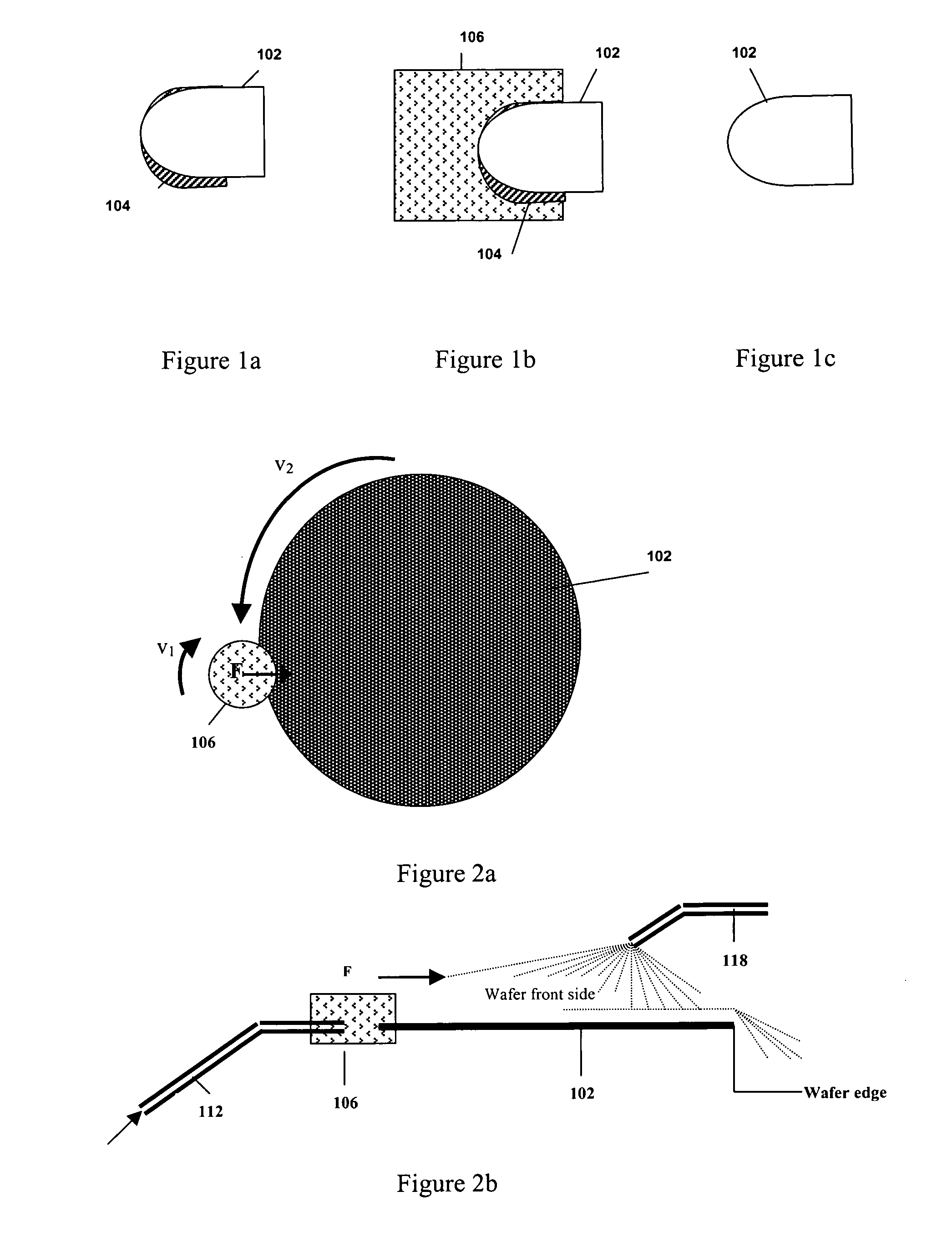
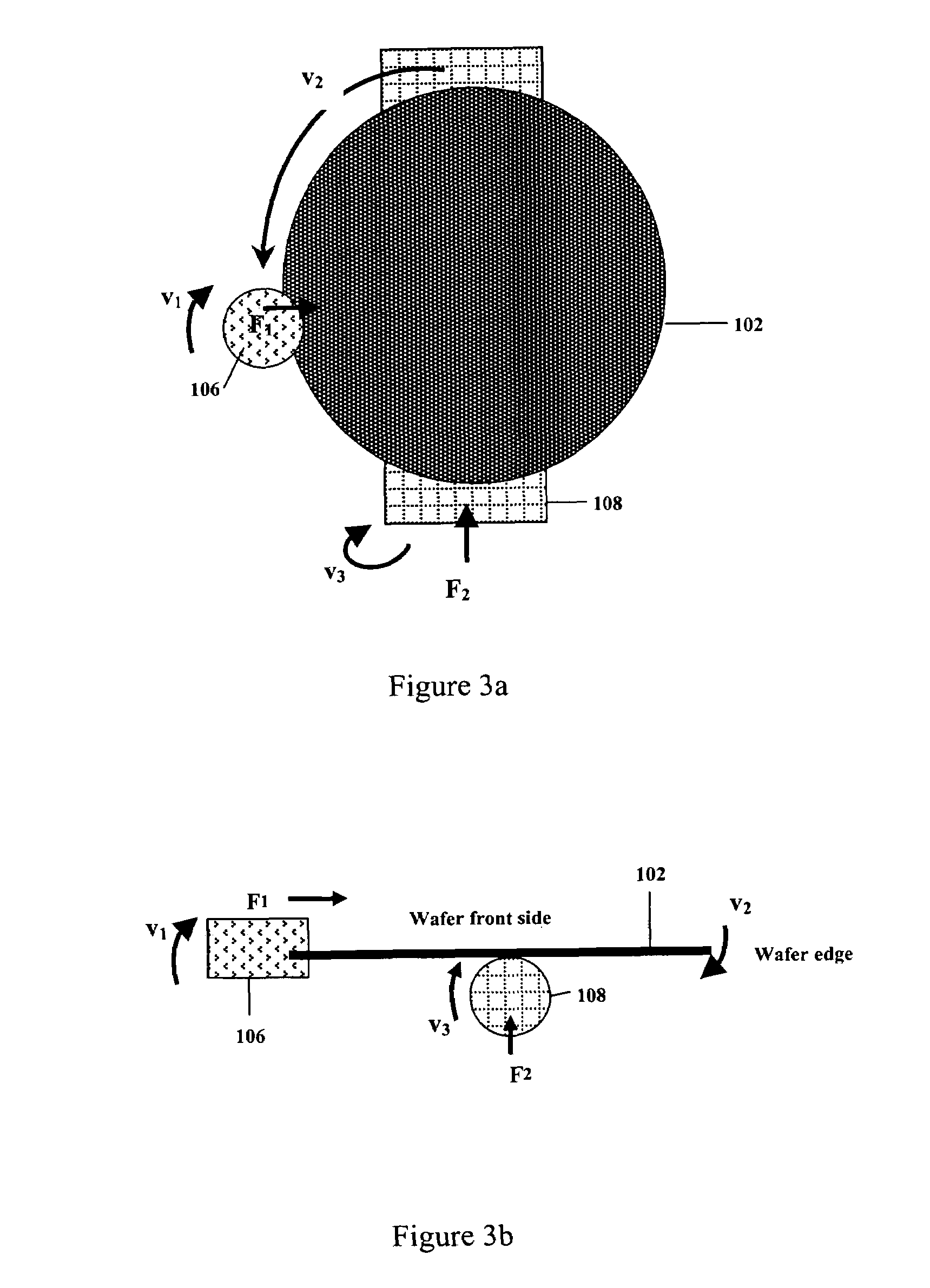
[0023]Several embodiments for an improved and more effective wafer edge cleaning apparatus, system and method will now be described. It will be obvious, however, to one skilled in the art, that the present invention may be practiced without some or all of these specific details. In other instances, well known process operations have not been described in detail in order not to unnecessarily obscure the present invention.
[0024]Wafer edge cleaning apparatus, systems and methods are very important to the ultimate quality of the resulting semiconductor products, e.g., microchips. In the present invention, the bevel polymers deposited on the wafer edges are treated with mechanical and chemical scrubbing that cuts, tears and removes the bevel polymers from the wafer edge.
[0025]In this document, the term wafer and substrate are used inter-changeably to refer to a thin slice of a semi-conductor material (usually silicon), from which microchips are made. The substrate can also be a flat pane...
PUM
| Property | Measurement | Unit |
|---|---|---|
| Abrasive | aaaaa | aaaaa |
| Circumference | aaaaa | aaaaa |
| Breakdown voltage | aaaaa | aaaaa |
Abstract
Description
Claims
Application Information
 - R&D Engineer
- R&D Manager
- IP Professional
- Industry Leading Data Capabilities
- Powerful AI technology
- Patent DNA Extraction
Browse by: Latest US Patents, China's latest patents, Technical Efficacy Thesaurus, Application Domain, Technology Topic, Popular Technical Reports.
© 2024 PatSnap. All rights reserved.Legal|Privacy policy|Modern Slavery Act Transparency Statement|Sitemap|About US| Contact US: help@patsnap.com