System for providing a continuous motion sequential lateral solidification for reducing or eliminating artifacts in overlap regions, and a mask for facilitating such artifact reduction/elimination

a technology of overlap region and sequential lateral solidification, which is applied in the field of system and mask for processing a thin film semiconductor material, can solve problems such as microstructural artifacts, and achieve the effect of reducing or eliminating artifacts

Inactive Publication Date: 2010-07-20
THE TRUSTEES OF COLUMBIA UNIV IN THE CITY OF NEW YORK
View PDF267 Cites 22 Cited by
  • Summary
  • Abstract
  • Description
  • Claims
  • Application Information

AI Technical Summary

Benefits of technology

[0006]An object of the present invention is to provide techniques for forming large-grained, grain-shaped and grain-boundary-location controlled polycrystalline thin film semiconductors using a sequential lateral solidification (“SLS”) process, and to reduce or eliminate artifacts.
[0007]According to the present invention, an arrangement, process and mask are provided for implementing single-scan continuous motion sequential lateral solidification of a thin film situated on a sample such that artifacts are reduced or eliminated. For example, according to the present invention artifacts that may be formed at the edges of the beamlets irradiating the thin film are significantly reduced. According to this invention, the edge areas of the previously irradiated and resolidified areas which likely have artifacts provided therein are overlapped by the subsequent beamlets. In this manner, the edge areas of the previously resolidified irradiated areas and artifacts therein are completely melted throughout their thickness. At least the subsequent beamlets are shaped such that the grains of the previously irradiated and resolidified areas which border the edge areas melted by the subsequent beamlets grow into these resolidifying edges areas so as to substantially reduce or eliminate the artifacts.
[0009]At least one first section of the first areas irradiated by at least one particular beamlet of the first beamlets is allowed to re-solidify and crystallize thereby having grains grown therein. The first section includes at least one first resolidified area irradiated by the one of the edge sections of the particular beamlet, the first resolidified area including artifacts therein. After the one or more first areas are irradiated, the second beamlets irradiate one or more second areas of the film sample so that the second areas are melted throughout their thickness. At least one second section of the second areas irradiated by the subsequent beamlet is allowed to re-solidify and crystallize thereby having grains grown therein. The second section includes at least one second resolidified area irradiated by the at least one of the edge sections of the subsequent beamlet which overlaps the artifacts provided in the first resolidified area. In this manner, the artifacts can thus be substantially reduced or even eliminated upon the resolidification of the second section of the second area.

Problems solved by technology

One problem that may arise during SLS processing of a thin film provided on a sample is microstructural artifacts, e.g., grain misalignment.

Method used


Image

  • System for providing a continuous motion sequential lateral solidification for reducing or eliminating artifacts in overlap regions, and a mask for facilitating such artifact reduction/elimination
  • System for providing a continuous motion sequential lateral solidification for reducing or eliminating artifacts in overlap regions, and a mask for facilitating such artifact reduction/elimination
  • System for providing a continuous motion sequential lateral solidification for reducing or eliminating artifacts in overlap regions, and a mask for facilitating such artifact reduction/elimination

Examples


Embodiment Construction

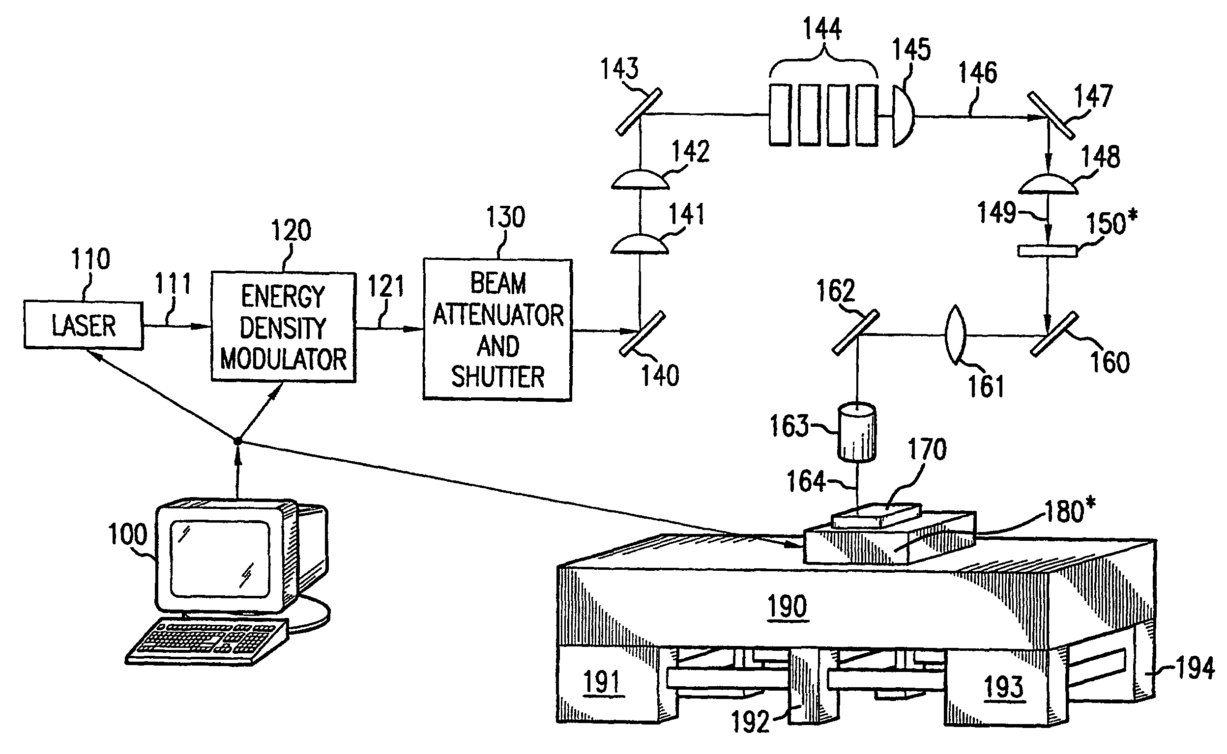
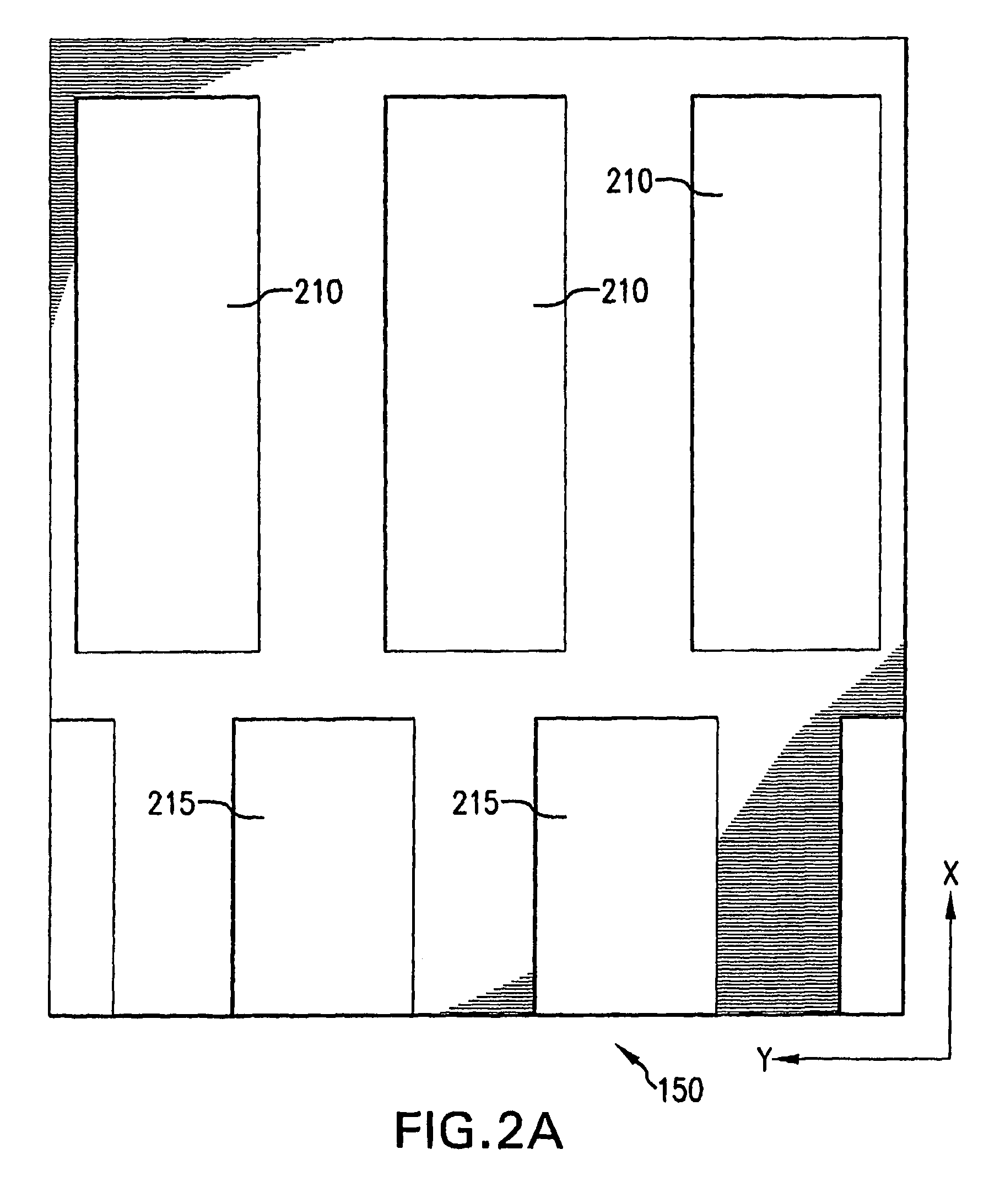
[0024]Certain systems and methods for providing a single scan, continuous motion SLS are described in International Publication No. 02 / 086954 (the “'954 Publication”), the entire disclosure of which is incorporated herein by reference. The '954 Publication explicitly describes and illustrates the details of these systems and methods, and their utilization of microtranslations of a sample, which may have an amorphous silicon thin film provided thereon that can be irradiated by irradiation beam pulses so as to promote the sequential lateral solidification on the thin film, without the need to microtranslate the sample and / or the beam relative to one another to obtain a desired length of the grains contained in the irradiated and re-solidified areas of the sample. Similar to the system described in the '954 Publication, an exemplary embodiment of a system for carrying out the continuous motion SLS processing of amorphous silicon thin films and reduce or eliminate microstructural artifa...


PUM

PropertyMeasurementUnit
widthaaaaaaaaaa
widthaaaaaaaaaa
thicknessaaaaaaaaaa

Abstract

An arrangement, process and mask for implementing single-scan continuous motion sequential lateral solidification of a thin film provided on a sample such that artifacts formed at the edges of the beamlets irradiating the thin film are significantly reduced. According to this invention, the edge areas of the previously irradiated and resolidified areas which likely have artifacts provided therein are overlapped by the subsequent beamlets. In this manner, the edge areas of the previously resolidified irradiated areas and artifacts therein are completely melted throughout their thickness. At least the subsequent beamlets are shaped such that the grains of the previously irradiated and resolidified areas which border the edge areas melted by the subsequent beamlets grow into these resolidifying edges areas so as to substantially reduce or eliminate the artifacts.

Description

CROSS-REFERENCE TO RELATED APPLICATIONS[0001]This application is a continuation of International Application Serial No. PCT / US04 / 030324, filed Sep. 16, 2004, published Mar. 31, 2005, which claims priority from U.S. Provisional Application Ser. No. 60 / 503,409, filed Sep. 16, 2003, each of which are incorporated by reference in their entireties herein, and from which priority is claimed.FIELD OF THE INVENTION[0002]The present invention relates to a method, system and mask for processing a thin-film semiconductor material, and more particularly to forming large-grained, grain-shaped and grain-boundary-location controlled semiconductor thin films from amorphous or polycrystalline thin films on a substrate by continuous motion-scanning the entire sample or at least one portion thereof using a sequential lateral solidification technique so as to reduce or even eliminate artifacts, e.g., that may be formed in overlapped irradiated, melted and resolidifying regions of a sample or in the por...

Claims


Application Information

Patent Timeline
Patent Type & Authority Patents(United States)
IPC IPC(8): H01L21/20H01L
CPCB23K26/0656B23K26/0676B23K26/073H01L21/02532H01L21/0268H01L21/02686H01L21/02691B23K26/066
Inventor IM, JAMES S.
Owner THE TRUSTEES OF COLUMBIA UNIV IN THE CITY OF NEW YORK
Why Eureka
Try Eureka