Circuit device and manufacturing method thereof

a technology of circuit devices and manufacturing methods, applied in the direction of printed circuit components, printed circuit manufacturing, printed circuit assembling, etc., can solve the problems of complex formation of contact holes 108/b>, the inability of the substrate to efficiently discharge heat generated by the embedded elements to the outside, etc., to reduce the planar size of the through hole thus formed, enhance the mechanical strength of the connecting portion, and enhance the reliability of the connecting portion

Active Publication Date: 2010-08-03
SEMICON COMPONENTS IND LLC
View PDF21 Cites 7 Cited by
  • Summary
  • Abstract
  • Description
  • Claims
  • Application Information

AI Technical Summary

Benefits of technology

[0012]According to the circuit device of the present invention, the first wiring layer is provided with the first connecting portion and the second wiring layer is provided with the second connecting portion. Moreover, the first connecting portion and the second connecting portion contact each other at an intermediate portion in the thickness direction of the insulating layer on which the first wiring layer and the second wiring layer are laminated. Therefore, it is possible to enhance reliability of the connecting portions against external force such as heat stress. Further, it is possible to enhance mechanical strength of the connecting portions by forming any of the first connecting portion and the second connecting portion integrally with the wiring layer by processing a copper foil.
[0013]According to the method of manufacturing a circuit device of the present invention, it is possible to form the via hole easily on the insulating layer by providing the though hole on the insulating layer which is thinly formed by burying the first connecting portion. Moreover, it is possible to reduce a planar size of the though hole thus formed. Furthermore, the plated film can be formed in the via hole easily because it is possible to form the shallow via hole.

Problems solved by technology

However, the organic substrate such as a glass epoxy substrate has low thermal conductivity, and therefore has a problem that the substrate cannot discharge heat generated by the embedded elements efficiently to the outside.
Moreover, there is also a problem that formation of the contact holes 108 is complicated when resin containing a large amount of inorganic filler is applied as the material of the support substrate 101 in order to enhance a heat radiation performance of the support substrate 101.

Method used


Image

  • Circuit device and manufacturing method thereof
  • Circuit device and manufacturing method thereof
  • Circuit device and manufacturing method thereof

Examples


first embodiment

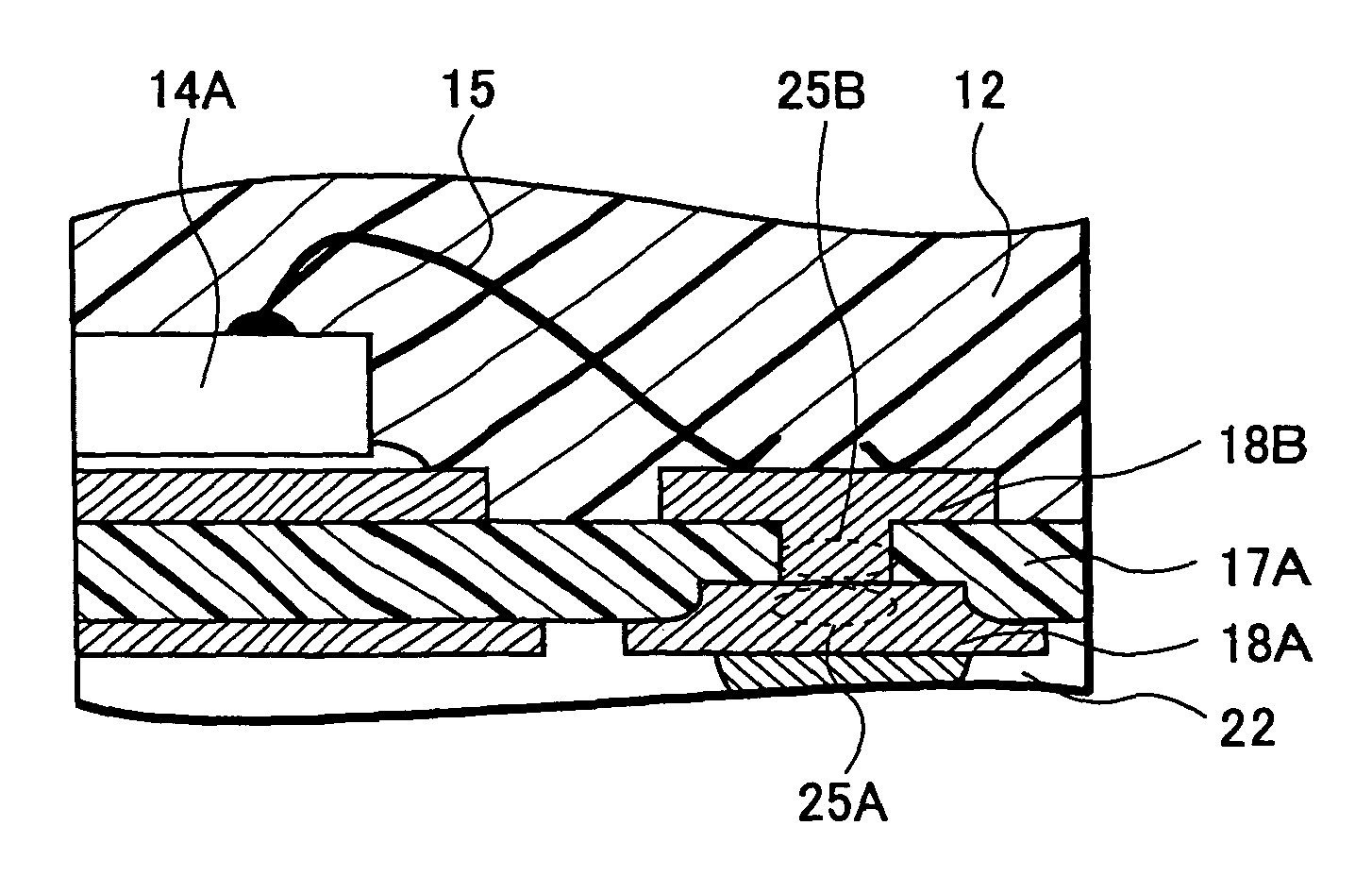
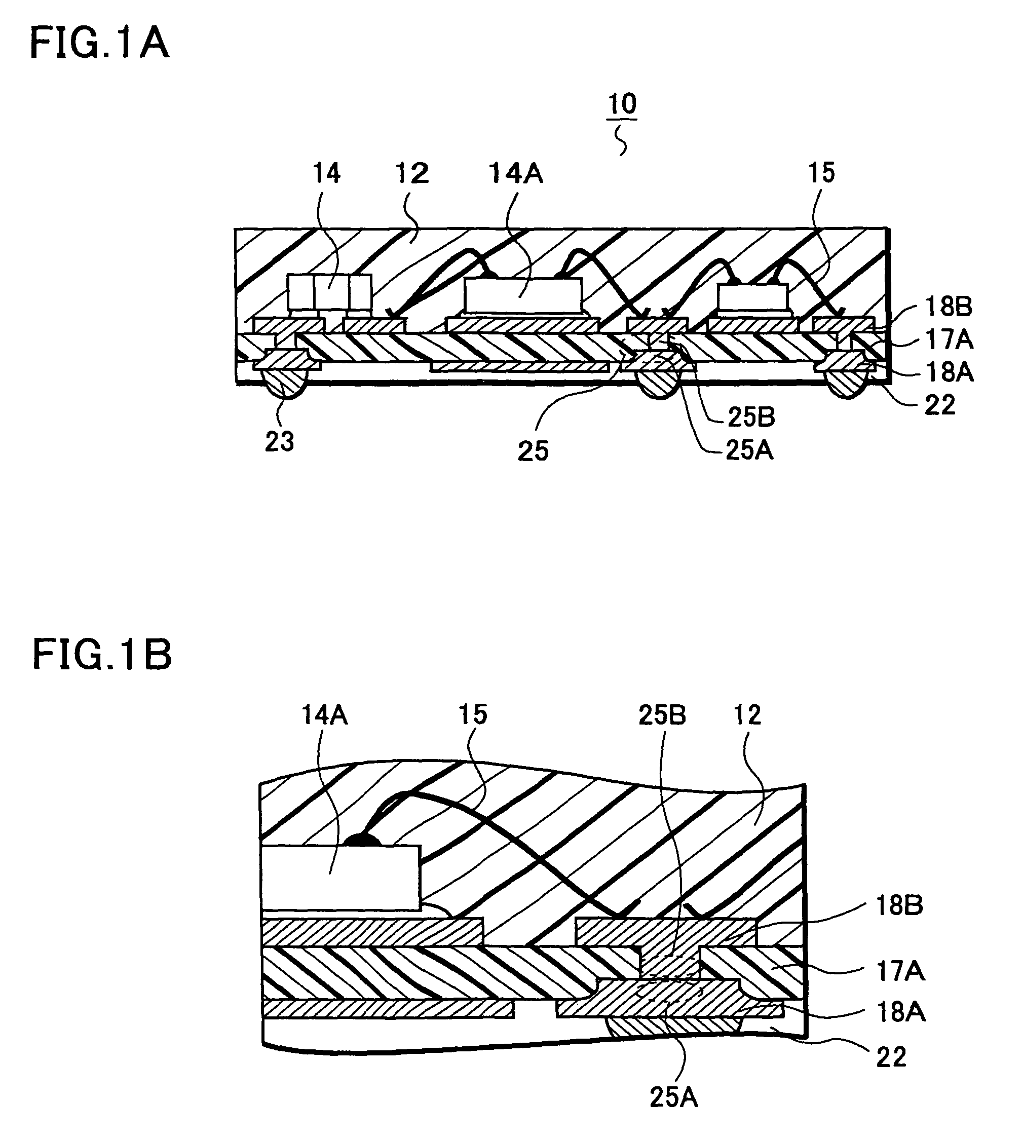
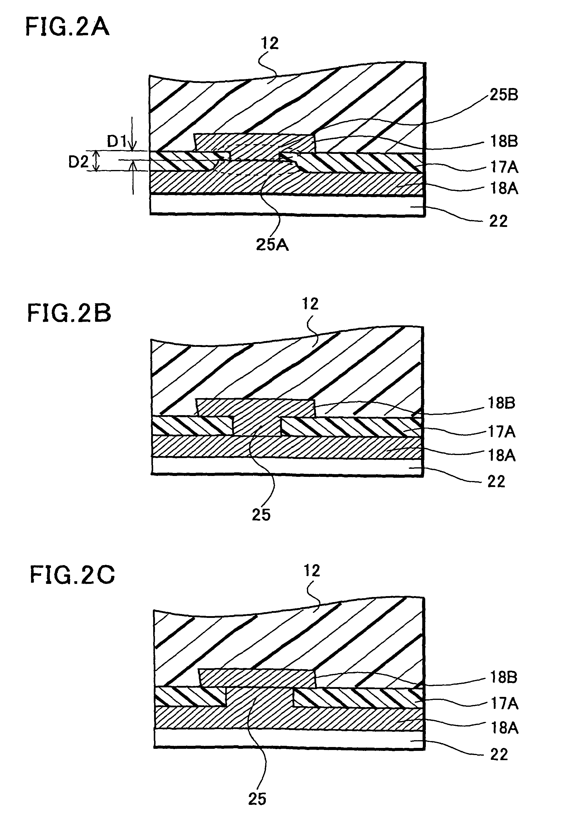
[0029]Circuit device 10 will be described with reference to FIGS. 1A and 1B. FIG. 1A is a cross-sectional view of the circuit device 10, and FIG. 1B is an enlarged cross-sectional view of connecting portion 25 of the circuit device 10 and the vicinity thereof.

[0030]A multilayer wiring structure including first wiring layer 18A and second wiring layer 18B is formed in the circuit device 10 of this embodiment. The second wiring layer 18B is laminated on the first wiring layer 18A while interposing first insulating layer 17A therebetween. The second wiring layer 18B which is an upper layer is electrically connected to circuit elements 14. External electrodes 23 are formed on a rear surface of the first wiring layer 18A located as a lower layer. Moreover, the circuit elements 14 and the second wiring layer 18B are covered with sealing resin 12. The circuit device 10 having the above-described schematic configuration will be described below in detail.

[0031]The first wiring layer 18A is m...

second embodiment

[0064]In this embodiment, a manufacturing method will be explained while taking the above-described circuit device 10 as an example. It is to be noted, however, that the following manufacturing method of this embodiment is also applicable to methods of manufacturing the circuit devices of other types.

[0065]Firstly, first conductive film 28A is prepared as shown in FIG. 5A. As the first conductive film 28A, it is possible to apply a material containing copper as a main component and a material containing Fe—Ni or Al as a main component. In terms of a thickness of the first conductive film 28A, it is required to provide a thickness equal to or above a sum of the thickness of the wiring layer 18A expected to be formed and a height of first connecting portion 25A. To be more precise, the thickness of the first conductive film 28A is set in a range from about 20 μm to 150 μm. Resist 29 covers a surface of the first conductive film 28A in regions where the first connecting portions 25A ar...


PUM


Abstract

A circuit device including a multilayer wiring structure having an improved heat radiation performance, and a manufacturing method thereof is provided. A circuit device of the invention includes a first wiring layer and a second wiring layer laminated while interposing a first insulating layer. The first wiring layer is connected to the second wiring layer in a desired position through a connecting portion formed so as to penetrate the first insulating layer. The connecting portion includes a first connecting portion protruding in a thickness direction from the first wiring layer, and a second connecting portion protruding in the thickness direction from the second wiring layer. The first connecting portion and the second connecting portion contact each other at an intermediate portion in the thickness direction of the insulating layer.

Description

BACKGROUND OF THE INVENTION[0001]Priority is claimed to Japanese Patent Application Number JP2004-193290 filed on Jun. 30, 2004, the disclosure of which is incorporated herein by reference in its entirety.[0002]1. Field of the Invention[0003]The present invention relates to a circuit device and a manufacturing method thereof, more specifically, to a circuit device including a plurality of wiring layers laminated while interposing an insulating layer, and a manufacturing method thereof[0004]2. Background Art[0005]A configuration of conventional circuit device 100 will be described with reference to FIG. 15. This technology is described for instance in Japanese Patent Publication No. 2001-339151 (p. 1, FIG. 1). FIG. 15 is a cross-sectional view of the conventional circuit device 100.[0006]In the conventional circuit device 100, first conductive pattern 102A is formed on a surface of support substrate 101 and second conductive pattern 102B is formed on a rear surface of the support sub...

Claims


Application Information

Patent Timeline
Patent Type & Authority Patents(United States)
IPC IPC(8): H01L23/48H01L23/52H01L29/40H01L23/04H01L23/10H01L23/34
CPCH01L23/3128H05K3/4647H01L23/5384H01L2924/10253H01L2221/68377H01L2224/48091H01L2224/48465H01L2224/73265H01L2924/01046H01L2924/01078H01L2924/01079H01L2924/13055H01L2924/15311H01L2924/19041H01L2924/19105H05K2201/0355H05K2201/09509H05K2201/09563H05K2203/0369H05K2203/0733H05K2203/1476H01L2924/1305H01L2924/13034H01L24/48H01L2224/32225H01L2224/73204H01L2224/92247H01L2924/1301H01L2924/00014H01L2924/00H01L2924/14H01L2924/181H01L2224/16225H01L2224/73253H01L2924/16152H01L2924/00012H01L2224/45099H01L2224/45015H01L2924/207H01L27/00H05K3/34
Inventor IGARASHI, YUSUKENAKAMURA, TAKESHIINOUE, YASUNORIUSUL, RYOSUKEMIZUHARA, HIDEKI
Owner SEMICON COMPONENTS IND LLC
Why Eureka
Try Eureka