

Semiconductor device
a technology of semiconductors and devices, applied in the field of semiconductor devices, can solve problems such as increased plane area, and achieve the effect of reducing the plane area
- Summary
- Abstract
- Description
- Claims
- Application Information
AI Technical Summary
Benefits of technology
Problems solved by technology
Method used
Image

Examples
first embodiment
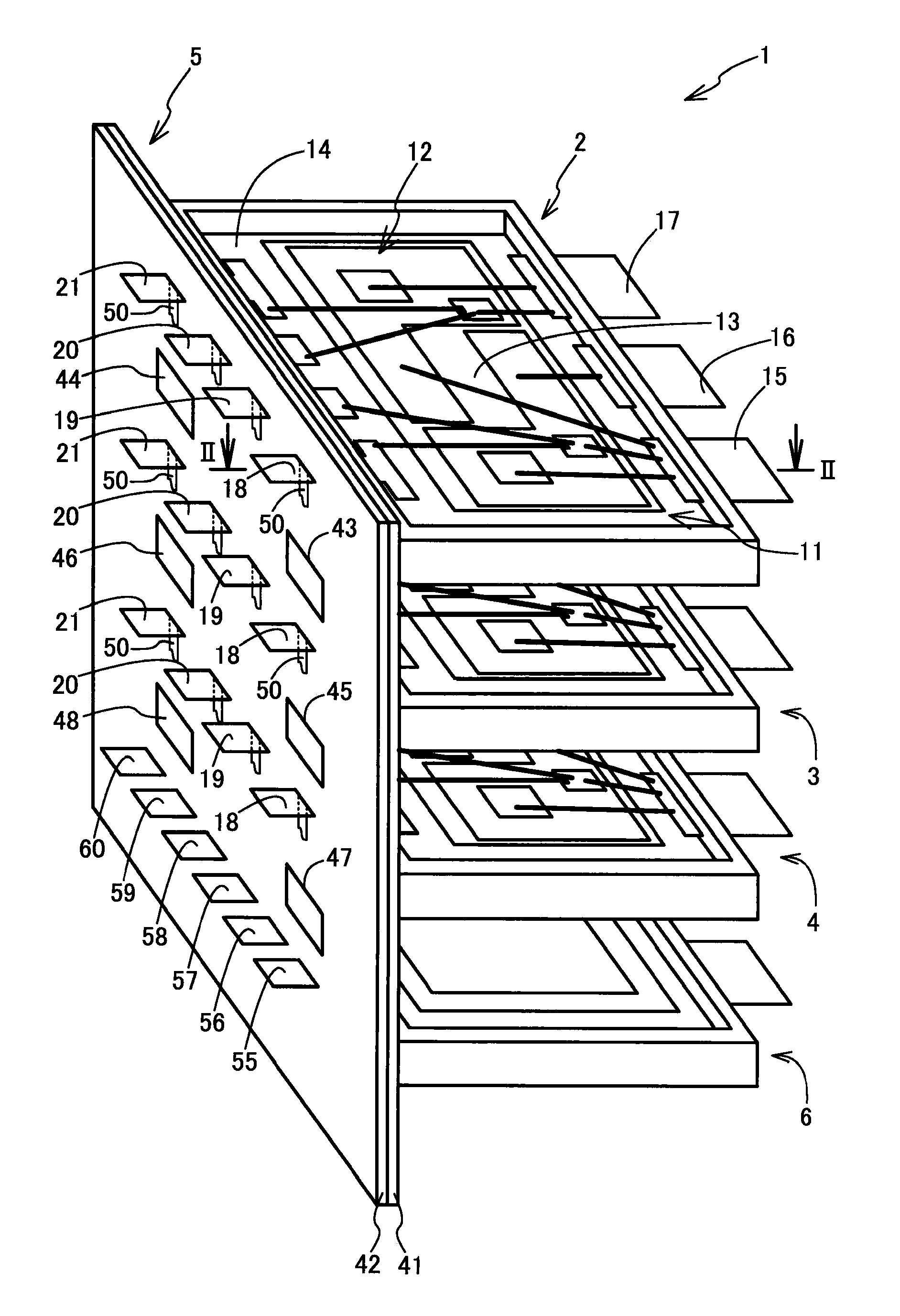
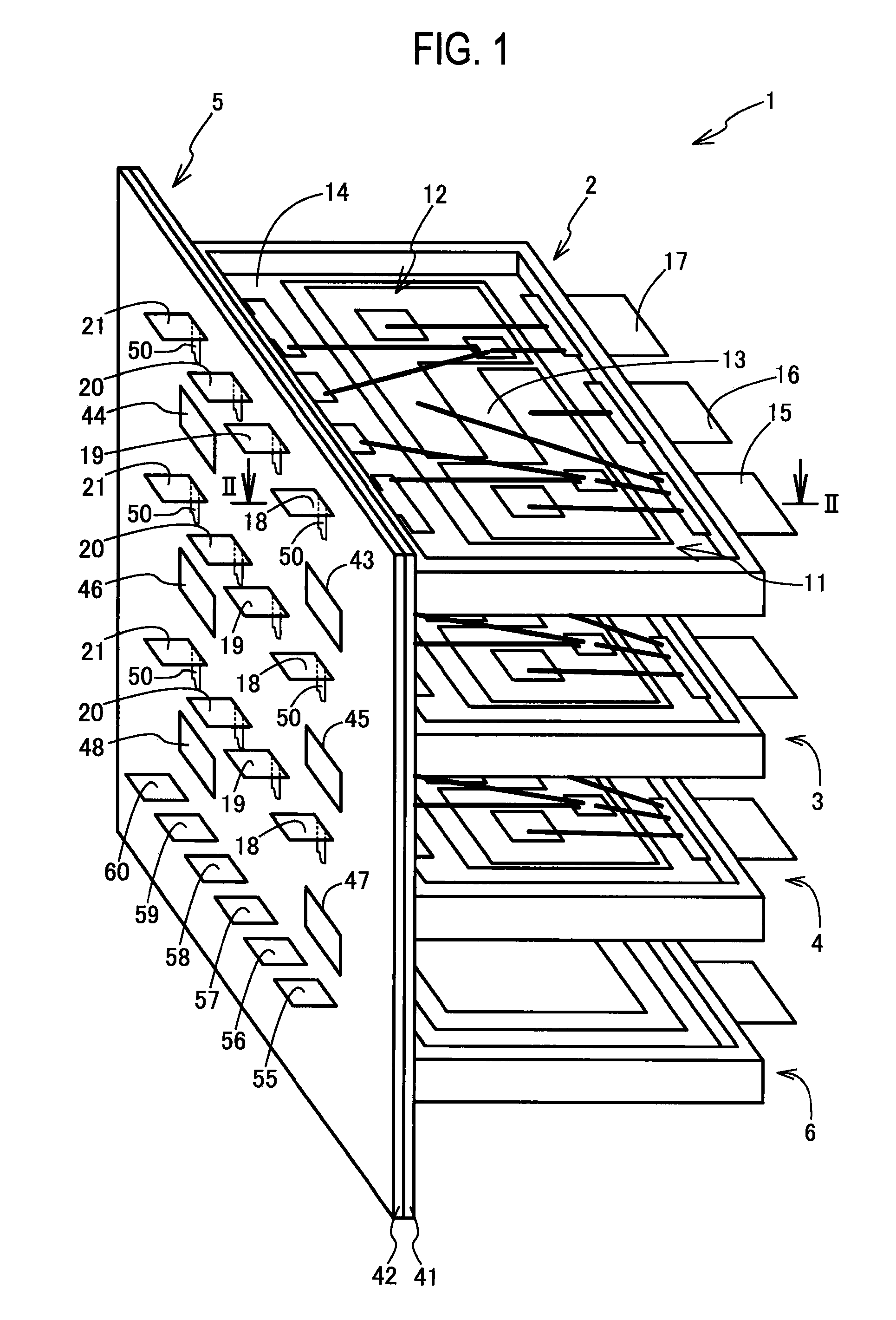
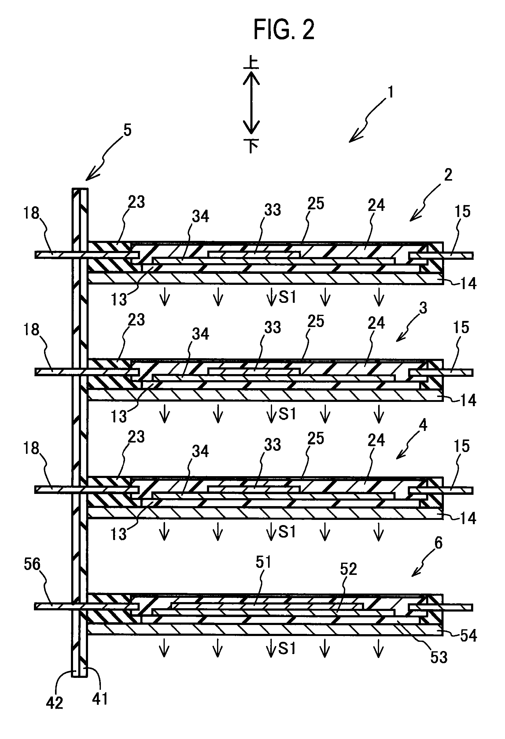
[0041]With reference to the drawings, description will be given of a first embodiment in which the present invention is applied to a three-phase intelligent power module (hereinafter referred to as an IPM). FIG. 1 is an overall perspective view of an IPM according to a first embodiment. FIG. 2 is a cross-sectional view along the line II-II in FIG. 1. FIG. 3 is a plan view of a U-phase output unit. FIG. 4 is a cross-sectional view along the line IV-IV in FIG. 3. FIG. 5 is a perspective view showing a switching device. FIG. 6 is a perspective view showing a diode. FIG. 7 is a schematic circuit diagram of the IPM. Note that, in the following description, “top” and “bottom” shown in FIG. 2 represent a vertical direction.
[0042]As shown in FIGS. 1 and 2, an IPM 1 according to the first embodiment includes a U-phase output unit 2, a V-phase output unit 3, a W-phase output unit 4, a controller 5 and a booster 6. The output units 2 to 4 configured to output different phases and the booster 6...
second embodiment
[0067]Next, description will be given of a second embodiment obtained by partially modifying the first embodiment described above. Note that the same constituent components as those of the first embodiment are denoted by the same reference numerals and description thereof will be omitted. FIG. 11 is a cross-sectional view equivalent to FIG. 2, showing an IPM according to the second embodiment. FIG. 12 is a plan view of an output unit on a high voltage unit side. FIG. 13 is a plan view of an output unit on a low voltage unit side.
[0068]As shown in FIG. 11, in an IPM 1A according to the second embodiment, output units 2A to 4A having high voltage units 11 and output units 2B to 4B having low voltage units 12 are formed of different components. Moreover, the output units 2A to 4A on the high voltage unit 11 side and the output units 2B to 4B on the low voltage unit 12 side are fixed to a controller 5A so as to be stacked on each other.
[0069]As shown in FIG. 12, the output unit 2A has a...
third embodiment
[0071]Next, description will be given of a third embodiment obtained by partially modifying the second embodiment described above. Note that the same constituent components as those of the first and second embodiments are denoted by the same reference numerals and description thereof will be omitted. FIG. 14 is a cross-sectional view equivalent to FIG. 2, showing an IPM according to the third embodiment.
[0072]As shown in FIG. 14, in an IPM 1B according to the third embodiment, the output units 2A to 4A on the high voltage unit 11 side in the IPM 1A in the second embodiment are turned upside down and mounted on the controller 5A. Specifically, the switching device 32 and the diode 33 in the high voltage unit 11 and the switching device 36 and the diode 37 in the low voltage unit 12 are arranged so as to face each other.
[0073]According to the configuration described above, parasitic inductances to be cancelled can be increased.
PUM
 Abstract
Description
Claims
Application Information