Manufacturing method of epitaxial structure of semiconductor

A technology of epitaxial structure and fabrication method, applied in semiconductor devices, electrical components, circuits, etc., can solve the problems of high material dislocation density and insufficient crystal quality of GaN materials, and achieve the effect of reducing the plane area

Active Publication Date: 2018-11-23
GUANGDONG INST OF SEMICON IND TECH
View PDF4 Cites 4 Cited by
  • Summary
  • Abstract
  • Description
  • Claims
  • Application Information

AI Technical Summary

Problems solved by technology

[0006] In view of this, the object of the present invention is to provide a semiconductor epitaxial structure manufacturing

Method used


Image

  • Manufacturing method of epitaxial structure of semiconductor
  • Manufacturing method of epitaxial structure of semiconductor
  • Manufacturing method of epitaxial structure of semiconductor

Examples


Embodiment Construction

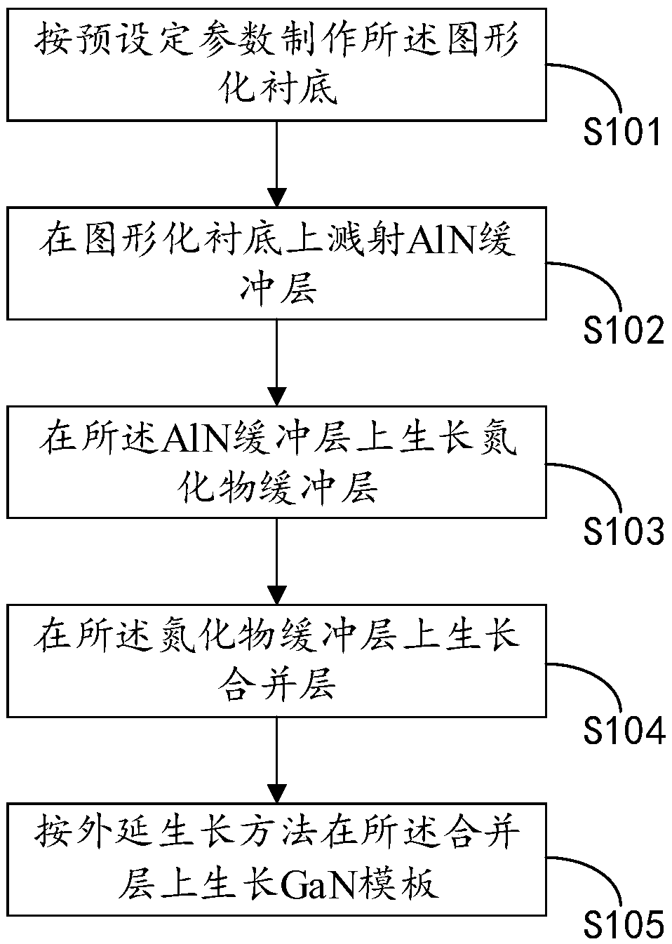
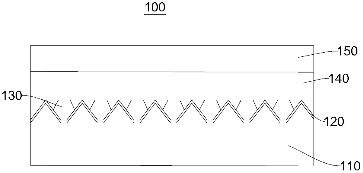
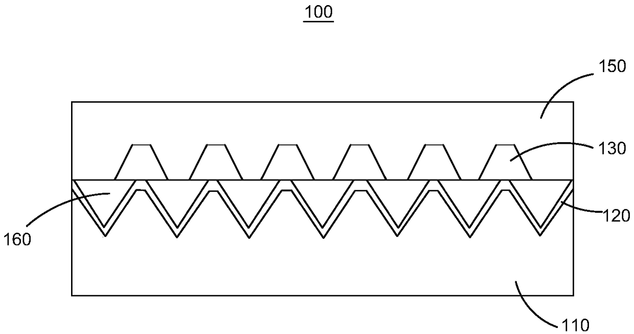
[0039] In order to make the purpose, technical solutions and advantages of the embodiments of the present invention clearer, the technical solutions in the embodiments of the present invention will be clearly and completely described below in conjunction with the drawings in the embodiments of the present invention. Obviously, the described embodiments It is a part of embodiments of the present invention, but not all embodiments. The components of the embodiments of the invention generally described and illustrated in the figures herein may be arranged and designed in a variety of different configurations.

[0040] The following will clearly and completely describe the technical solutions in the embodiments of the present invention with reference to the accompanying drawings in the embodiments of the present invention. Obviously, the described embodiments are only some, not all, embodiments of the present invention. The components of the embodiments of the invention generally ...


PUM

PropertyMeasurementUnit
Thicknessaaaaaaaaaa
Thicknessaaaaaaaaaa

Abstract

The invention provides a manufacturing method of an epitaxial structure of a semiconductor, and relates to the technical field of semiconductors. First, an AlN buffer layer is sputtered on a pre-set patterned substrate, wherein the surface of the patterned substrate comprises a plurality of regular hexagonal structures arranged periodically, the regular hexagonal structures are arranged accordingto preset parameters, the regular hexagonal structures comprise regular hexagonal bottom faces and cones connected to the bottom faces, and the bottom faces are parallel to the c-faces of a substratematerial; a nitride buffer layer then grows on the AlN buffer layer; the nitride buffer layer grows along the c-faces between the cones of every two adjacent regular hexagonal structures; and finally,a nitride merged layer grows on the nitride buffer layer. The manufacturing method of the epitaxial structure of the semiconductor has the effects of improving the flatness of the surface of the semiconductor, reducing the dislocation density of the semiconductor and enabling the quality of crystal lattice to be better.

Description

technical field [0001] The invention relates to the technical field of semiconductors, in particular to a method for manufacturing a semiconductor epitaxial structure. Background technique [0002] At present, due to the advantages of high efficiency, energy saving, environmental protection, and long life, LEDs have received widespread attention. [0003] Generally, LED lighting is a white light source scheme that uses blue LEDs to excite yellow or other phosphor technology, in which blue LEDs mainly use InGaN / GaN quantum wells for excitation, mainly including n-type electron injection layers grown on GaN templates, InGaN / GaN quantum well active region, p-type hole injection layer and other optimized structures to improve quantum efficiency, and the crystal quality of GaN template will seriously affect the subsequent growth of n-type layer, quantum well, p-type layer and other crystals of all subsequent epitaxial layers Quality, and the crystal quality of epitaxy is one of...

Claims


Application Information

Patent Timeline
IPC IPC(8): H01L33/22H01L33/12H01L33/00
CPCH01L33/0066H01L33/0075H01L33/12H01L33/22
Inventor 张康赵维陈志涛贺龙飞何晨光吴华龙廖乾光
Owner GUANGDONG INST OF SEMICON IND TECH
Why Eureka
Try Eureka