Quad flat pack in quad flat pack integrated circuit package system

a quad-flat pack, integrated circuit technology, applied in the direction of electrical equipment, semiconductor devices, semiconductor/solid-state device details, etc., can solve the problems of insufficient cooling and reliability concerns, current packaging suppliers are struggling to accommodate high-speed computer devices, and no clear cost-effective technology has yet been identified

Active Publication Date: 2010-08-17
STATS CHIPPAC LTD
View PDF5 Cites 4 Cited by
  • Summary
  • Abstract
  • Description
  • Claims
  • Application Information

AI Technical Summary

Problems solved by technology

Current packaging suppliers are struggling to accommodate the high-speed computer devices that are projected to exceed one TeraHertz (THz) in the near future.
The current technologies, materials, equipment, and structures offer challenges to the basic assembly of these new devices while still not adequately addressing cooling and reliability concerns.
The envelope of technical capability of next level interconnect assemblies are not yet known, and no clear cost effective technology has yet been identified.
These challenges demand not only automation of manufacturing, but also the automation of data flow and information to the production manager and customer.
The limitations and issues with current technologies include increasing clock rates, EMI radiation, thermal loads, second level assembly reliability stresses and cost.
As these package systems evolve to incorporate more components with varied environmental needs, the pressure to push the technological envelope becomes increasingly challenging.
More significantly, with the ever-increasing complexity, the potential risk of error increases greatly during manufacture.
Solutions to these problems have been long sought but prior developments have not taught or suggested any solutions and, thus, solutions to these problems have long eluded those skilled in the art.

Method used


Image

  • Quad flat pack in quad flat pack integrated circuit package system
  • Quad flat pack in quad flat pack integrated circuit package system
  • Quad flat pack in quad flat pack integrated circuit package system

Examples


first embodiment

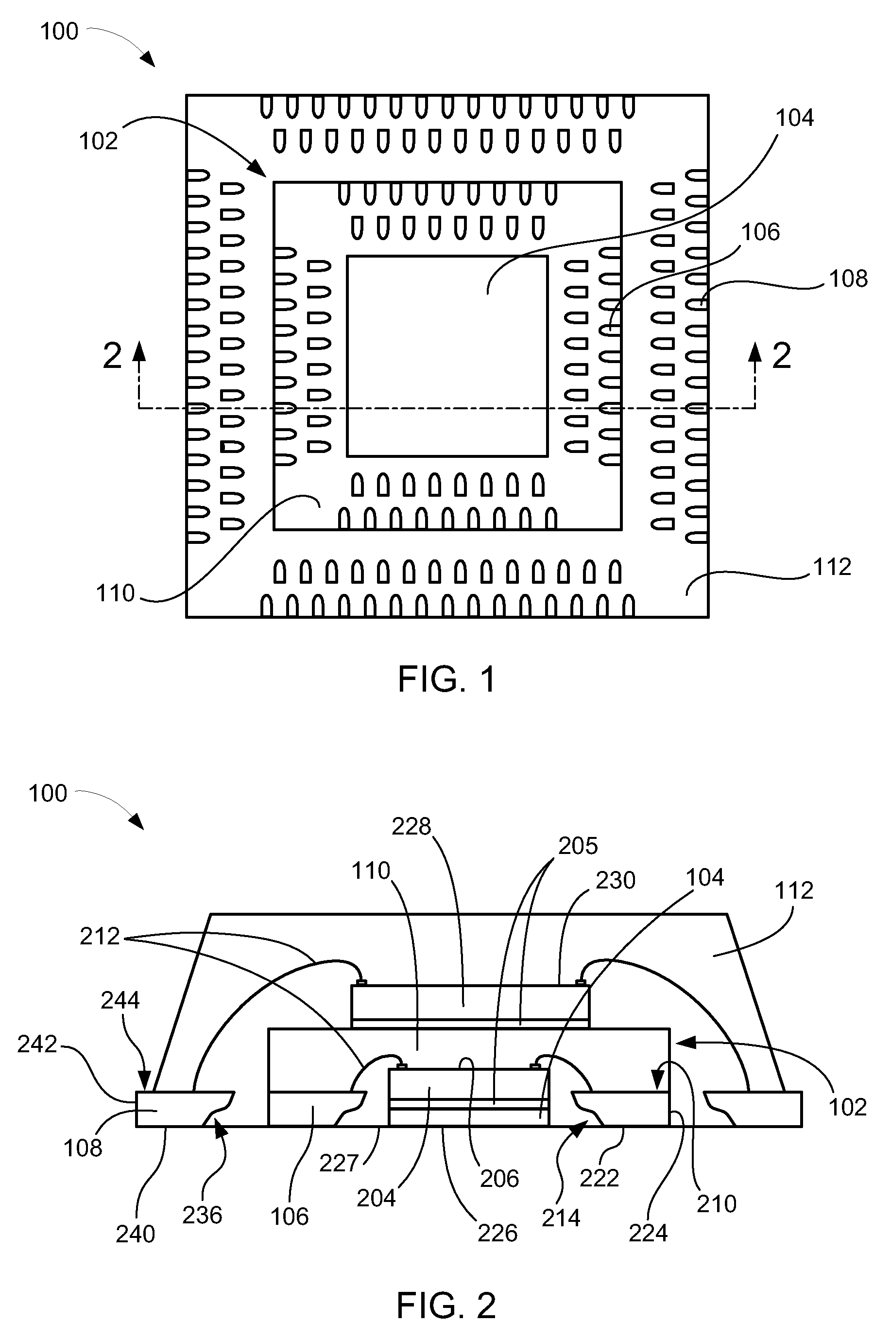
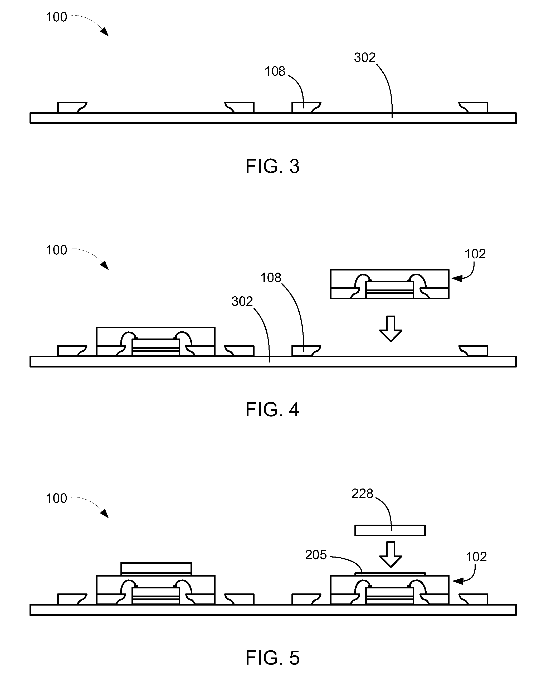
[0041]Referring now to FIG. 1, therein is shown a bottom view of an integrated circuit package system 100 in the present invention. The integrated circuit package system 100 is shown having a base package 102 such as a quad flat pack with no leads (QFN).

[0042]The base package 102 has a die-pad 104. The base package 102 has inner leads 106 on the periphery of the die-pad 104. On the periphery of the base package 102, outer leads 108 are mounted.

[0043]The inner leads 106 and the die-pad 104 are partially encapsulated by an inner encapsulation 110. The base package 102 along with the outer leads 108 are further partially encapsulated by an outer encapsulation 112.

[0044]Referring now to FIG. 2, therein is shown a cross-sectional view of the integrated circuit package system 100 along the line 2-2 of FIG. 1. The integrated circuit package system 100 is shown having the base package 102 containing a first integrated circuit 204, such as a wire-bonded die, with an active side 206.

[0045]The...

second embodiment

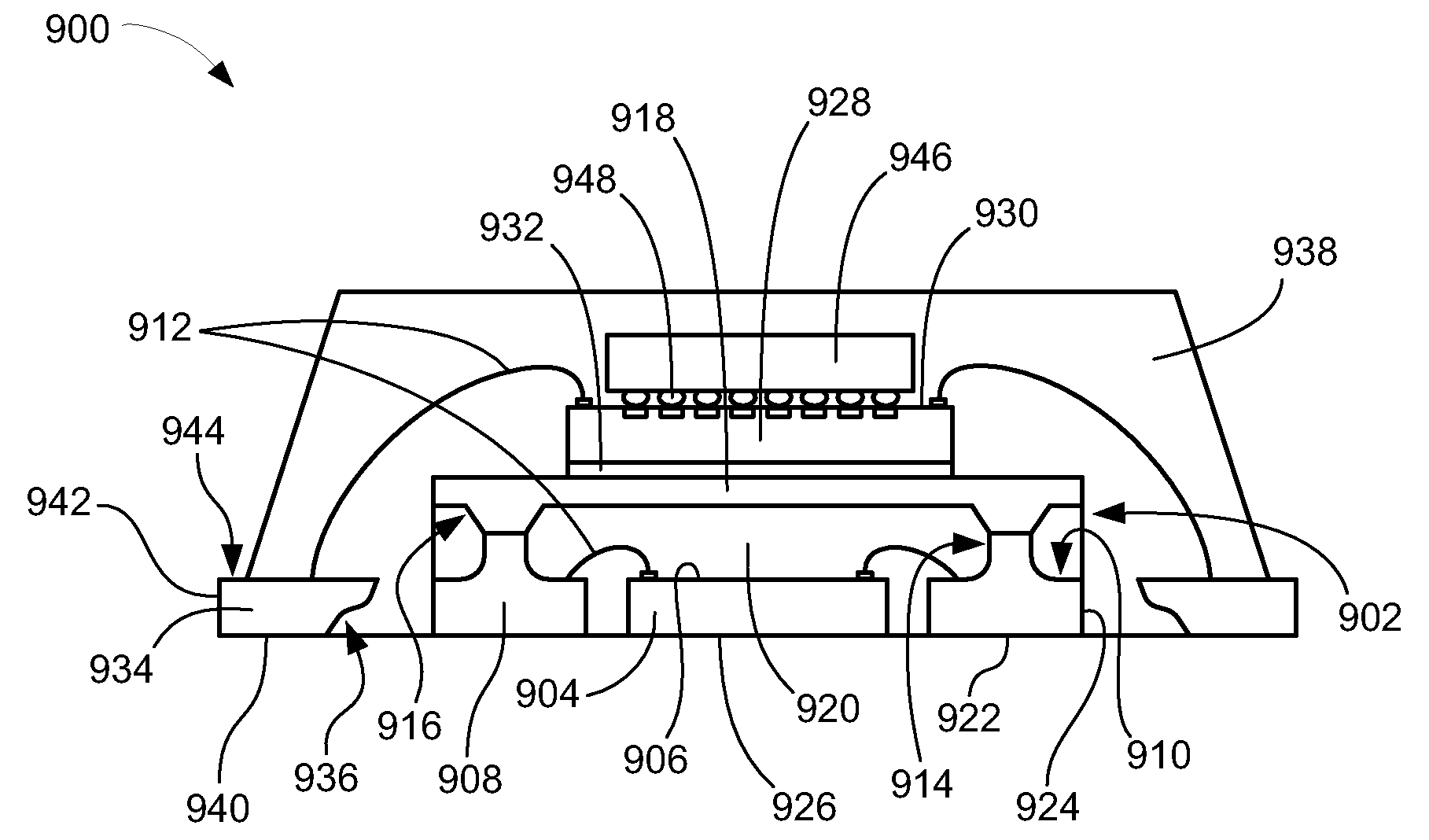
[0061]Referring now to FIG. 9, therein is shown a cross-sectional view of an integrated circuit package system 900 in the present invention. The integrated circuit package system 900 is shown having a base package 902 such as a quad flat pack with no leads (QFN).

[0062]The base package 902 has a first integrated circuit 904, such as a wire-bonded die, with an active side 906. Inner leads 908 surround the periphery of the first integrated circuit 904. The inner leads 908 have a top portion 910.

[0063]The active side 906 of the first integrated circuit 904 is connected to the top portion 910 of the inner leads 908 with bond wires 912. The inner leads 908 have lead extensions 914, which extend upward from the top portion 910 of the inner leads 908.

[0064]The lead extensions 914 correspond to and contact heat sink supports 916. The heat sink supports 916 extend downward from a heat sink 918. The heat sink 918 is highly thermally conductive to dissipate heat generated by the first integrate...


PUM


Abstract

An integrated circuit package system includes: providing a base package having a first integrated circuit with an inner lead on a periphery thereof and connected thereto with interconnects, and the inner lead partially encapsulated by an inner encapsulation; mounting an outer lead on the periphery of the base package; mounting a second integrated circuit above the base package and connected to the outer lead with the interconnects; and partially encapsulating, the base package and the outer leads with an outer encapsulation leaving a bottom surface of the inner lead and a bottom surface of the outer lead exposed.

Description

TECHNICAL FIELD[0001]The present invention relates generally to integrated circuits and more particularly to a system for utilizing a quad flat pack in a quad flat pack for a package in package system.BACKGROUND ART[0002]The rapidly growing portable electronics market, e.g. cellular phones, laptop computers, and PDAs, are an integral facet of modern life. The multitude of portable devices represents one of the largest potential market opportunities for next generation packaging. These devices have unique attributes that have significant impacts on manufacturing integration, in that they must be generally small, lightweight, and rich in functionality and they must be produced in high volumes at relatively low cost.[0003]As an extension of the semiconductor industry, the electronics packaging industry has witnessed ever-increasing commercial competitive pressures, along with growing consumer expectations and the diminishing opportunities for meaningful product differentiation in the m...

Claims


Application Information

Patent Timeline
Patent Type & Authority Patents(United States)
IPC IPC(8): H01L23/02
CPCH01L21/568H01L21/6835H01L23/3107H01L23/4334H01L23/49548H01L23/49575H01L24/97H01L25/03H01L25/50H01L24/83H01L24/16H01L24/28H01L24/48H01L24/81H01L24/85H01L2224/16145H01L2224/48091H01L2224/48247H01L2224/73265H01L2224/81801H01L2224/83192H01L2224/85001H01L2224/97H01L2924/01027H01L2924/01082H01L2924/078H01L2924/14H01L2924/3025H01L2224/83H01L2224/85H01L2924/00014H01L2924/01033H01L2224/32245H01L2924/00H01L2924/181H01L2224/32225H01L2924/18165H01L2224/85005H01L24/73H01L2224/04042H01L2924/00011H01L2924/00012H01L2224/0401H01L2224/45099H01L2224/45015H01L2924/207
Inventor MERILO, DIOSCORO A.DIMAANO, JR., ANTONIO B.
Owner STATS CHIPPAC LTD
Why Eureka
Try Eureka