

Chip package structure and circuit board thereof
a technology of chip package and circuit board, which is applied in the direction of printed circuit manufacturing, printed circuit stress/warp reduction, printed circuit aspects, etc., can solve the problems of reducing the area available for disposing circuit layers, reducing yield, and poor product reliability, so as to reduce the probability of trace pulling apart
- Summary
- Abstract
- Description
- Claims
- Application Information
AI Technical Summary
Benefits of technology
Problems solved by technology
Method used
Image

Examples
first embodiment
The First Embodiment
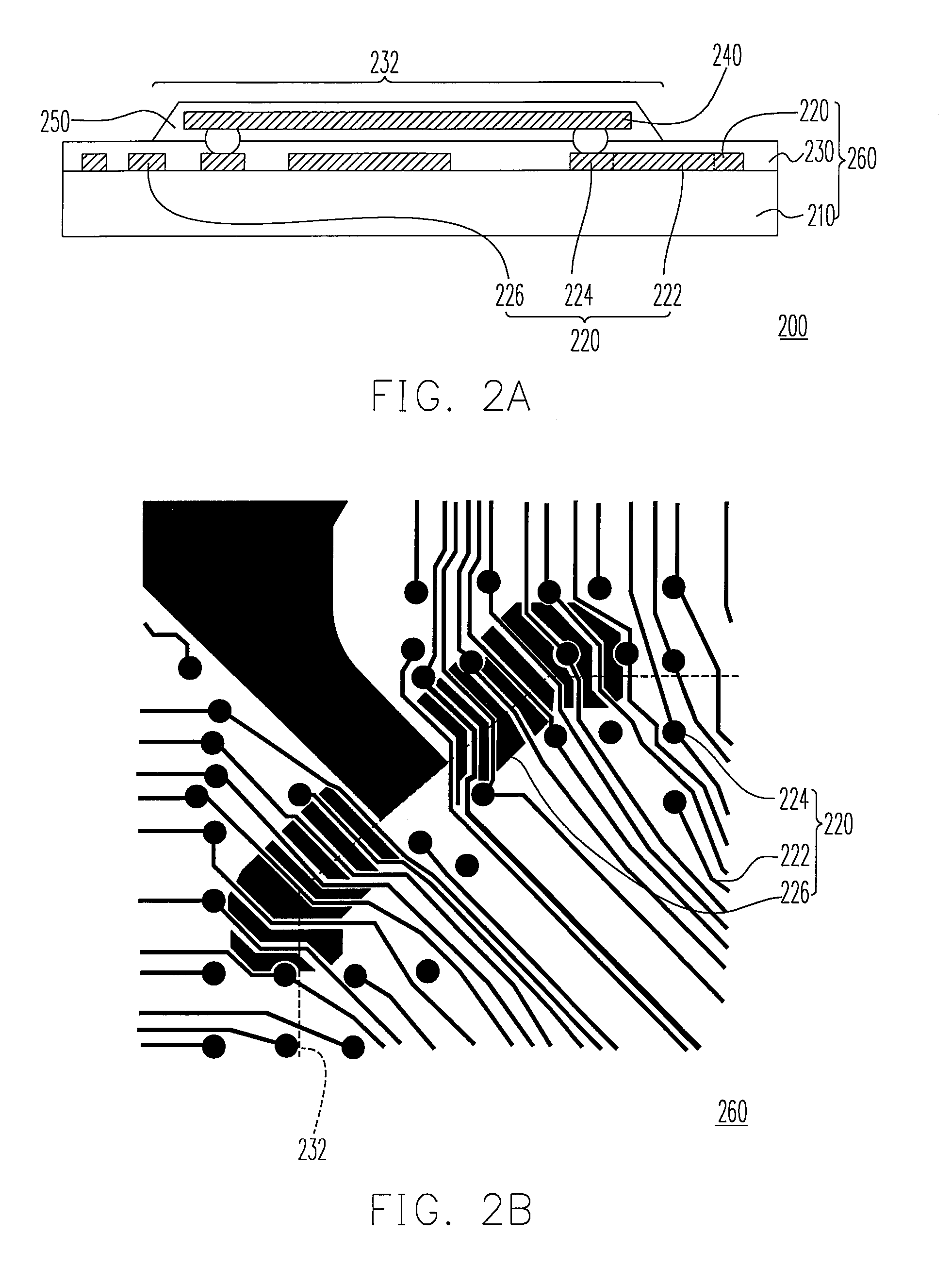
[0037]FIG. 2A is a schematic sectional view of a chip package structure having a circuit board according to a first embodiment of the present invention, and FIG. 2B is a schematic top view of a corner of the circuit board according to the first embodiment of the present invention. Referring to FIGS. 2A and 2B, the chip package structure 200 includes a circuit board 260, a chip 240, and an encapsulant 250. The circuit board 260 includes a substrate 210, a circuit layer 220, and a solder mask 230. The circuit layer 220 is disposed on the substrate 210 and includes a plurality of traces 222, a plurality of via holes 224, and a dummy trace 226. The dummy trace 226 is located between two adjacent traces 222, and the dummy trace 226 is electrically isolated from the traces 222 and the via holes 224. Moreover, the materials of the dummy trace 226, the traces 222, and the via holes 224 are, for example, the same conductive material, so as to form the traces 222, the via ...
second embodiment
The Second Embodiment
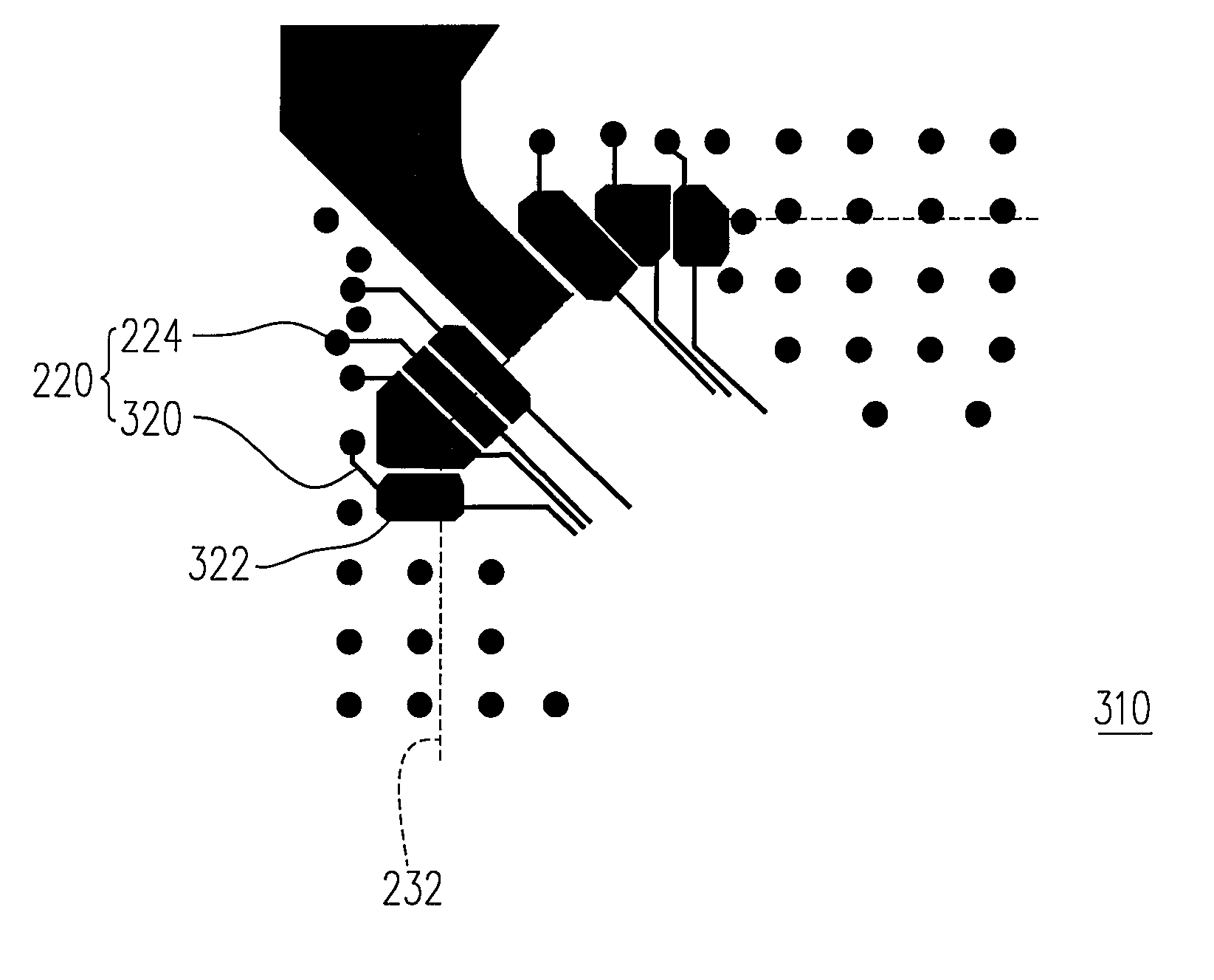
[0040]FIG. 4A is a schematic sectional view of a chip package structure having a circuit board according to a second embodiment of the present invention, and FIG. 4B is a schematic top view of a corner of the circuit board according to the second embodiment of the present invention. Referring to FIGS. 4A and 4B, a chip package structure 300 and a circuit board 310 thereof in the second embodiment are substantially the same as the chip package structure 200 and the circuit board 260 thereof in the first embodiment respectively, except that the chip package structure 300 and the circuit board 310 thereof do not have the dummy trace 226, but one trace 320 has an enlarged section 322 instead. A line width A of the enlarged section 322 of the trace 320 is larger than a line width B of the other portion of the trace 320.
[0041]Since the enlarged section 322 increases the contact area of the circuit layer 220 and the substrate 210, in which the circuit layer 220 is disp...
PUM
 Abstract
Description
Claims
Application Information