Power gating circuit, system on chip circuit including the same and power gating method

a power gating circuit and circuit technology, applied in the field of memory devices, can solve the problems of degrading the performance of the system-on-a-chip circuit, abnormal operation of adjacent logic circuits, and limited current (power) available for adjacent logic circuit operations, so as to reduce the peak current

Active Publication Date: 2010-08-24
SAMSUNG ELECTRONICS CO LTD
View PDF5 Cites 12 Cited by
  • Summary
  • Abstract
  • Description
  • Claims
  • Application Information

AI Technical Summary

Benefits of technology

[0008]An aspect of the present invention provides a power gating method for reducing the peak current that is applied to the memory device.
[0009]Some exemplary embodiments of the present invention provide a power gating circuit capable of reducing a peak current that is applied to a memory device.
[0010]Some exemplary embodiments of the present invention provide a system-on-a-chip circuit including a power gating circuit capable of reducing a peak current that is applied to a memory device.
[0011]Some exemplary embodiments of the present invention provide a power gating method for reducing a peak current that is applied to a memory device.
[0024]Therefore, accordingly a power gating circuit, a system-on-a-chip circuit which includes the power gating circuit, and a power gating method can disperse the peak current by turning ON three power gating transistors one after the other based on gradually increasing the voltage level on an internal power supply voltage bus. The gradual increase of the voltage level on the internal power supply voltage bus can reduce the influence of the peak current on adjacent intellectual properties. The term “intellectual properties” refers to devices made on a chip from plans selected from a library of pre-designed system level cores to accelerate the development process and to meet rapid product development schedules.

Problems solved by technology

The large current flows produce heat and may have adversely affect adjacent logic circuits, thereby degrading performance of the system-on-a-chip circuit.
If the peak current flowing into the memory device 110 is abruptly increased, the current (power) available for operations of the adjacent logic circuits may be limited such that the adjacent logic circuits may operate abnormally.

Method used


Image

  • Power gating circuit, system on chip circuit including the same and power gating method
  • Power gating circuit, system on chip circuit including the same and power gating method
  • Power gating circuit, system on chip circuit including the same and power gating method

Examples


Embodiment Construction

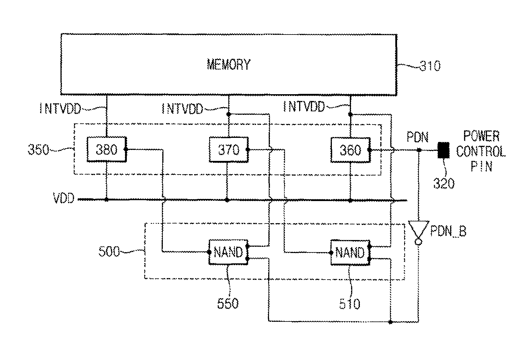
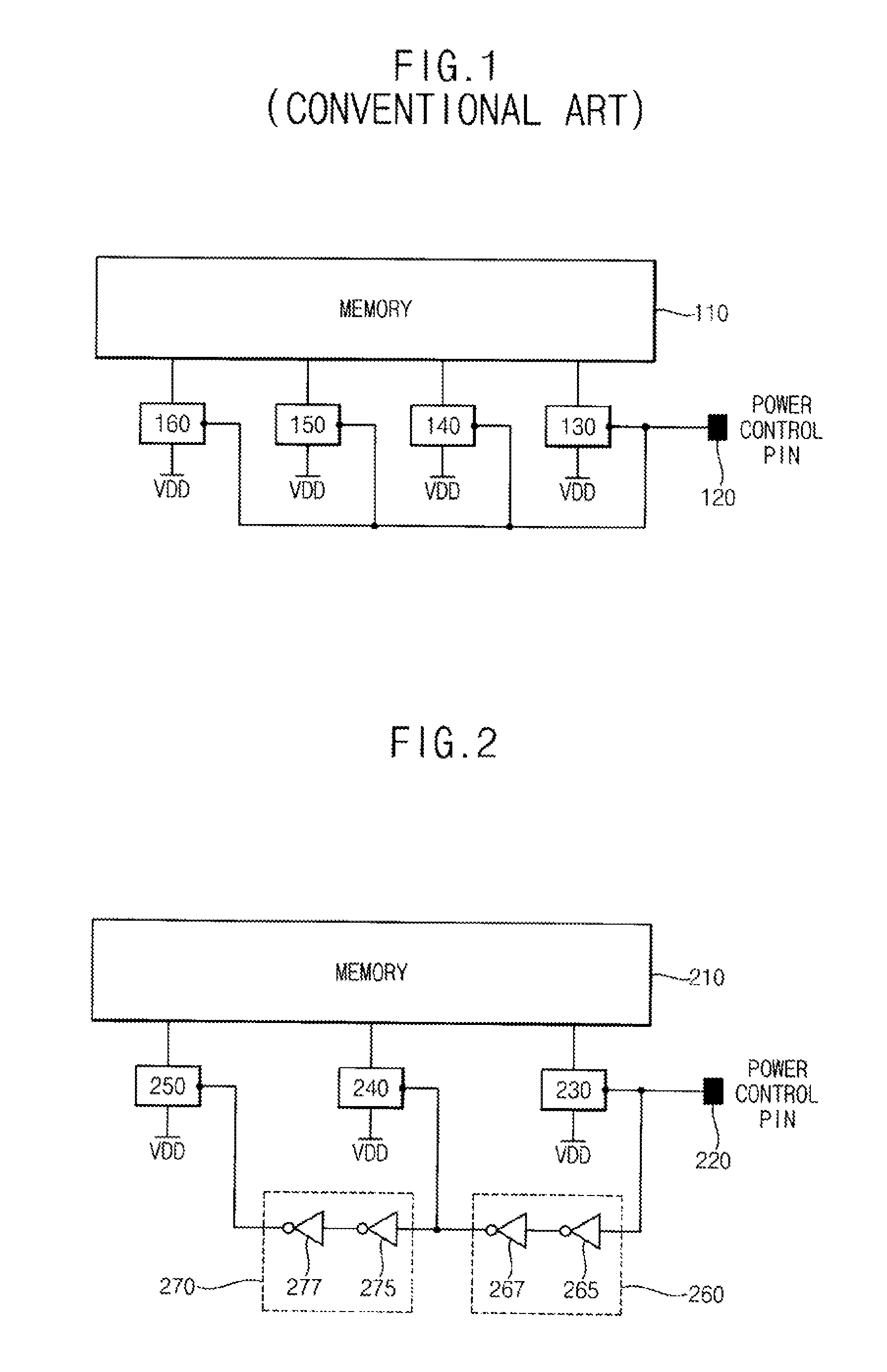
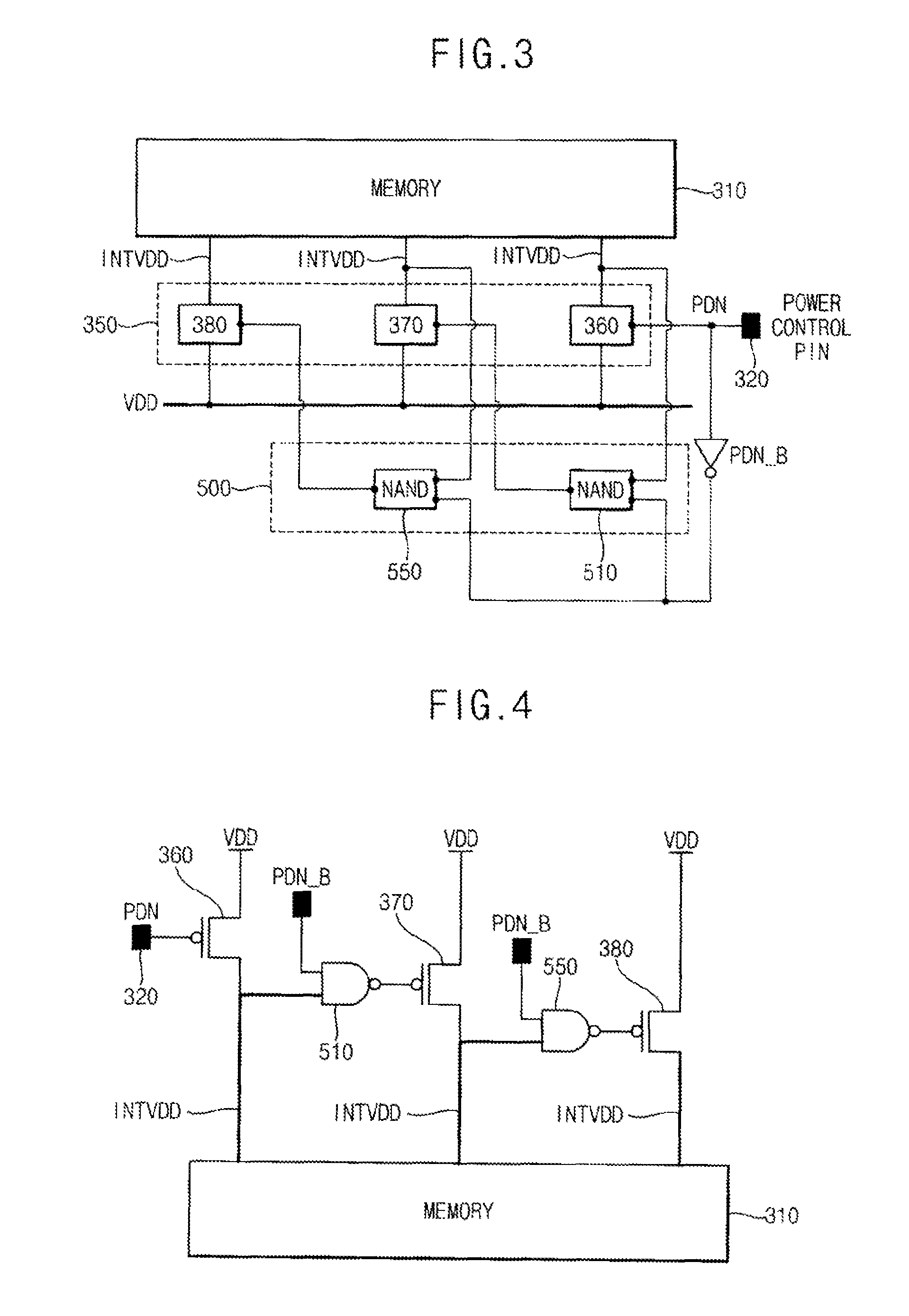
[0038]FIG. 2 is a block diagram illustrating a power gating circuit for a memory device 210 including an inverter delay chain 260 and 270.

[0039]Referring to FIG. 2, the power gating circuit includes a power control pin 220, power gating transistors 230, 240 and 250, a first inverter delay chain 260, and a second inverter delay chain 270. The first inverter delay chain 260 includes inverters 265 and 267. The second inverter delay chain 270 includes inverters 275 and 277.

[0040]When the first power gating transistor 230 is turned ON by a power control signal that is applied to the power control pin 220, a power supply voltage VDD is applied to a first pin of the memory device 210. When the second power gating transistor 240 is turned ON by the power control signal that is delayed through the first inverter chain 260, the power supply voltage VDD is applied to the first and second pin of the memory device 210. When the third power gating transistor 250 is turned ON by the power control ...


PUM


Abstract

A power gating circuit of a memory device includes a power gating unit and a control unit. The power gating unit includes first, second, and third power gating transistors connected in parallel between a power supply voltage and an internal power supply voltage bus of the memory device. The three power gating transistors are sequentially turned ON. The second and third power gating transistors turn ON sequentially in response to the increasing voltage level of the bus. The timing points when the second and third power gating transistors are sequentially turned ON is based upon detecting the gradually increasing the voltage level of the internal power supply voltage. The size of the first power gating transistor may be smaller than the size of the second power gating transistor, and the size of the second power gating transistor may be smaller than the size of the third power gating transistor.

Description

CROSS-REFERENCE TO RELATED APPLICATIONS[0001]This application claims priority under, 35 USC § 119, to Korean Patent Application No. 2006-0085417, filed on Sep. 6, 2006 in the Korean Intellectual Property Office (KIPO), which is incorporated by reference herein in its entirety.BACKGROUND OF THE INVENTION[0002]1. Field of the Invention[0003]The present invention relates to a memory device, and more particularly to a power gating circuit of a memory device, a system-on-a-chip (SoC) circuit including the power gating circuit, and a power gating circuit method for reducing a peak current.[0004]2. Description of the Related Art[0005]A typical system-on-a-chip (SoC) circuit consists of one or more microcontroller, microprocessor or DSP cores, memory blocks a ROM and a RAM, timing sources including oscillators and phase-locked loops, voltage regulators and power management circuits. When electric power is applied to a memory device included in a system-on-a-chip circuit, a relatively large ...

Claims


Application Information

Patent Timeline
Patent Type & Authority Patents(United States)
IPC IPC(8): G11C5/14
CPCG11C5/14H03K19/0016H03K3/356104
Inventor SEO, DONG-WOOKJUNG, JONG-HOONPARK, IN-GYULEE, CHAN-HO
Owner SAMSUNG ELECTRONICS CO LTD
Why Eureka
Try Eureka