Semiconductor memory device for reducing peak current during refresh operation

a memory device and memory technology, applied in the field of semiconductor memory devices, can solve the problems of reducing the charge quantity stored in the capacitor, however, as time passes, and achieve the effect of reducing the peak curren

Active Publication Date: 2008-04-15
SK HYNIX INC
View PDF22 Cites 13 Cited by
  • Summary
  • Abstract
  • Description
  • Claims
  • Application Information

AI Technical Summary

Benefits of technology

[0024]It is, therefore, an object of the present invention to provide a semiconductor memory device for reducing peak current during a refresh operation.

Problems solved by technology

Charge quantity stored in the capacitor, however, reduces as time passes.

Method used


Image

  • Semiconductor memory device for reducing peak current during refresh operation
  • Semiconductor memory device for reducing peak current during refresh operation
  • Semiconductor memory device for reducing peak current during refresh operation

Examples


Embodiment Construction

[0031]Hereinafter, a semiconductor memory device in accordance with the present invention will be described in detail referring to the accompanying drawings.

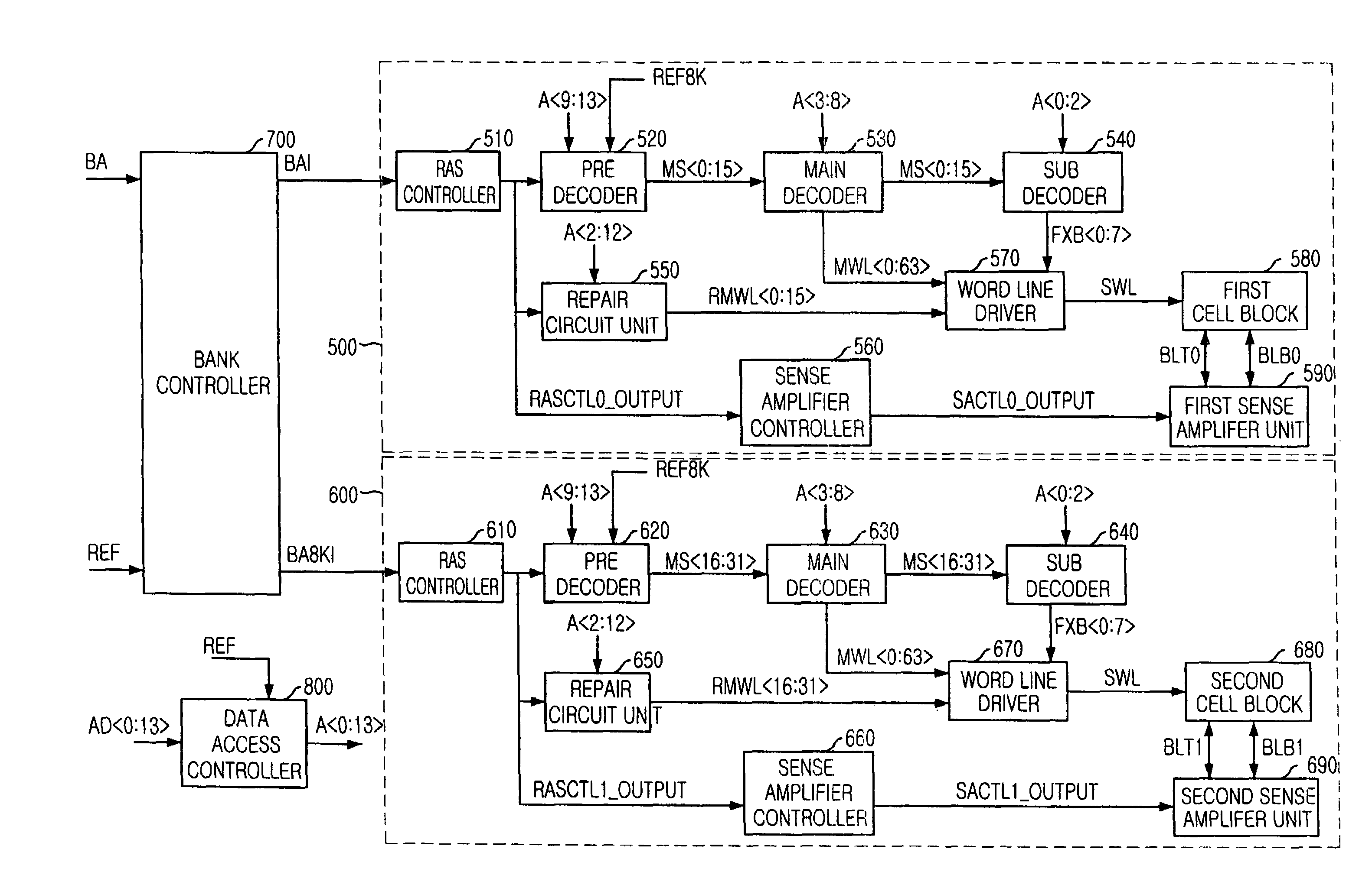
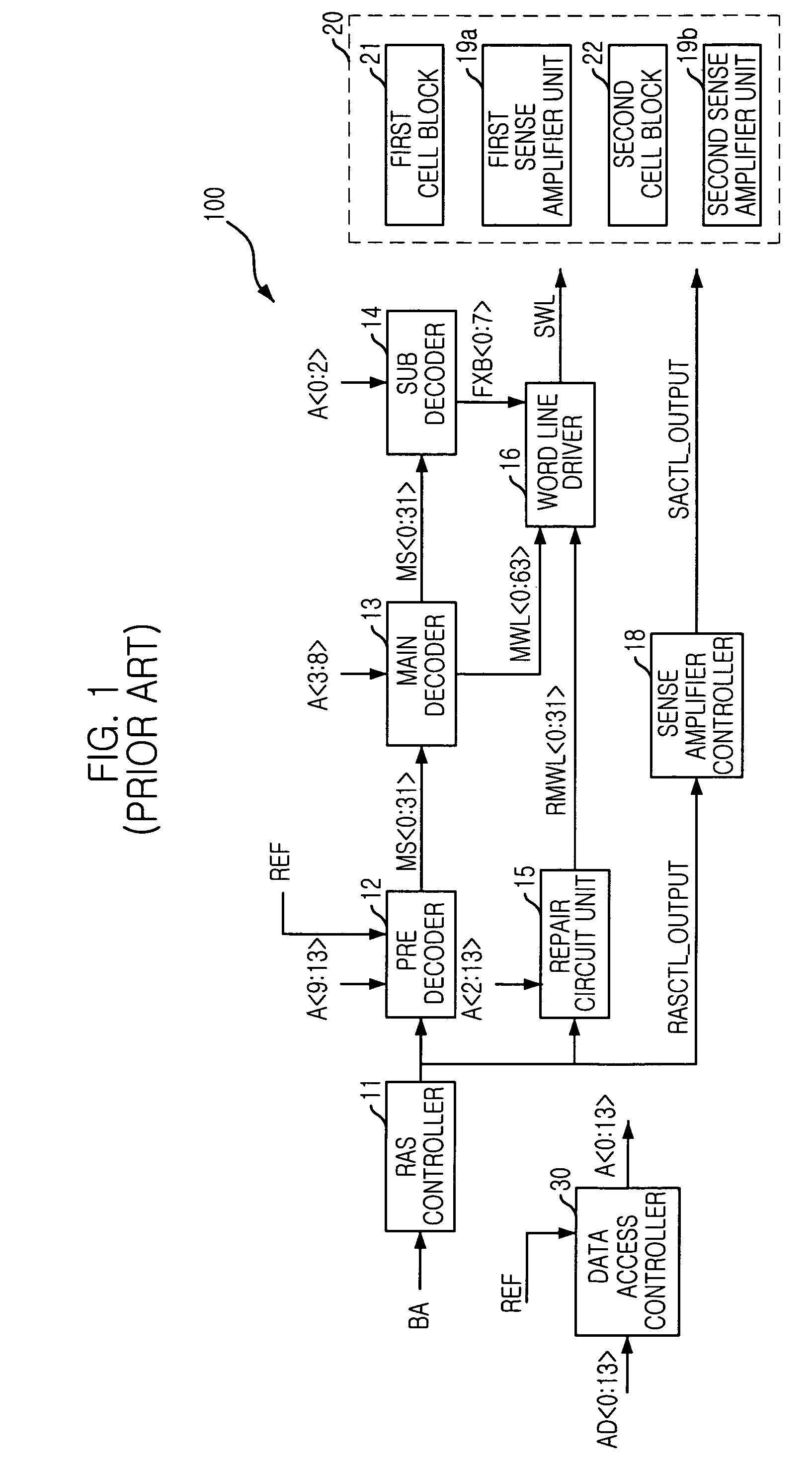
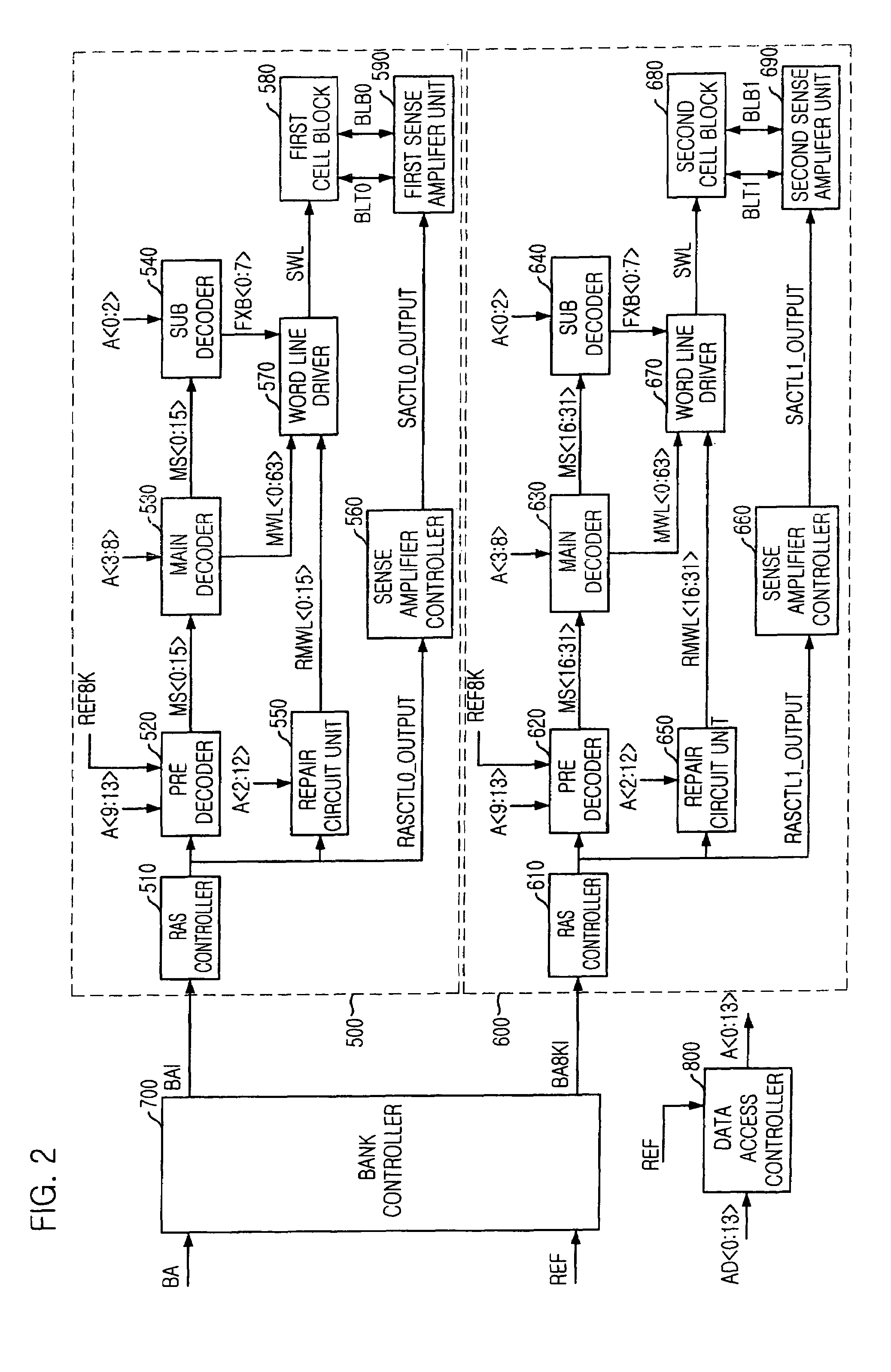
[0032]FIG. 2 is a block diagram showing a semiconductor memory device in accordance with the present invention.

[0033]As shown, the semiconductor memory device includes a first cell mat 500, a second cell mat 600, a data access controller 800 and a bank controller 700.

[0034]Each of the first cell mat 500 and the second cell mat 600 includes 8×1024 word lines. The data access controller 800 activates a word line of the first cell mat 500 or the second cell mat 600 at a data access operation; however, at a refresh operation, the data access controller 800 activates a word line of the first cell mat 500 and a word line of the second cell mat 600.

[0035]The bank controller 700 enables the first cell mat 500 and the second cell mat 600. At the data access operation, the bank controller 700 enables both of the first cell mat 500 and the...


PUM


Abstract

A semiconductor memory device comprises a plurality of banks, each having first and second cell mats, each having a plurality of word lines; a data access controller for selecting a word line from the first cell mat and the second cell mat in response to the row address and a refresh signal to be used in a refresh operation; and a bank controller for sequentially enabling the first cell mat and the second cell mat in response to a bank address and the refresh signal.

Description

FIELD OF INVENTION[0001]The present invention relates to a semiconductor memory device; and, more particularly, to a semiconductor memory device reducing peak current during a refresh operation.DESCRIPTION OF PRIOR ART[0002]Generally, a semiconductor memory device has two different types, one is a dynamic random access memory (DRAM) and the other is a static random access memory (SRAM).[0003]Since a memory cell included in the SRAM is formed by four latched transistors, the SRAM can hold its data without external refresh, for as long as power is supplied to the SRAM.[0004]In contrast, a memory cell included in the DRAM is formed by a transistor and a capacitor, and the capacitor has to be charged or discharged for the DRAM operation. Charge quantity stored in the capacitor, however, reduces as time passes. Therefore, the DRAM must be refreshed periodically in order to hold its data contents.[0005]Refresh operation for the DRAM is described below.[0006]A word line included in the DRA...

Claims


Application Information

Patent Timeline
Patent Type & Authority Patents(United States)
IPC IPC(8): G11C7/00G11C8/00G11C7/02G11C8/08G11C8/18G11C11/406
CPCG11C7/02G11C8/08G11C8/18G11C11/406G11C11/40618
Inventor YOU, MIN-YOUNG
Owner SK HYNIX INC
Why Eureka
Try Eureka