
Method for optimizing integrated circuit device design and service

Inactive Publication Date: 2010-08-31
INT BUSINESS MASCH CORP
View PDF9 Cites 17 Cited by
  • Summary
  • Abstract
  • Description
  • Claims
  • Application Information

AI Technical Summary

Benefits of technology

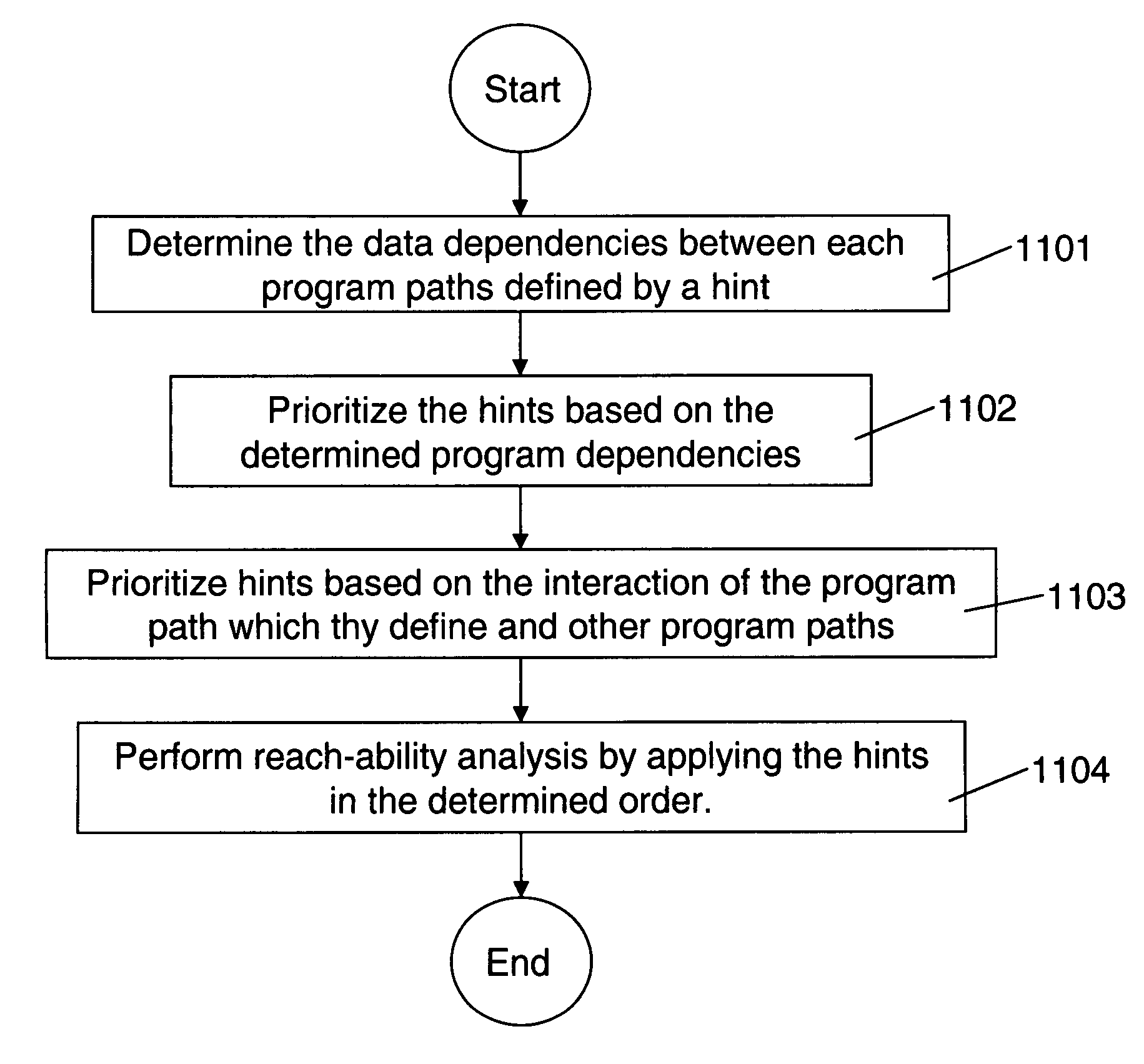
The present invention provides a method for automatically identifying a reasonable order in which to apply hints for performing reachability analysis of a program. This is important because the order in which hints are applied can affect the number of states reached. The method involves determining the order of application for each hint based on the interaction of the program paths defined by the hints. The invention also provides a data processing system and computer program product for performing this method. The technical effect of the invention is to improve the efficiency and accuracy of reachability analysis of programs.

Problems solved by technology

A problem associated with using hints to perform reach-ability analysis of a program is that the order in which the hints are applied will have an affect on the number of states reached and as a result a method is required which may be used to automatically identify a reasonable order in which to apply hints.

Method used


Image

  • Method for optimizing integrated circuit device design and service
  • Method for optimizing integrated circuit device design and service
  • Method for optimizing integrated circuit device design and service

Examples


Embodiment Construction

[0029]While the present invention will be described more fully hereinafter with reference to the accompanying drawings, in which a preferred embodiment of the present invention is shown, it is to be understood at the outset of the description which follows that persons of skill in the appropriate arts may modify the invention here described while still achieving the favorable results of the invention. Accordingly, the description which follows is to be understood as being a broad, teaching disclosure directed to persons of skill in the appropriate arts, and not as limiting upon the present invention. In particular, while the context for this disclosure is the design of integrated circuit devices, it is known that the “state explosion” problem here addressed is also found in software design and believed that the techniques and method here described will find usefulness in such applications.

[0030]The program analysis techniques employed to accomplish the objective outlined above are p...


PUM


Abstract

Improved analysis and refinement of integrated circuit device design and other programs is facilitated by methods in reach-ability analysis is performed using hints which define a particular path through a program. To ensure that a reasonable number of states are reached during reach-ability analysis a order to apply the hints is determined. The ordering prioritizes hints which define program paths which set a given variable over hints which define program slice which use the given variable.

Description

FIELD AND BACKGROUND OF INVENTION[0001]This invention relates to program analysis techniques, and in particular use of hints when performing program analysis, for example, a program which relates to an integrated circuit design.[0002]The design of integrated circuit devices conventionally uses hardware description languages (HDLs) to describe circuits (herein also sometimes called “systems”) at various levels of abstraction. As a circuit design evolves, designers and verification engineers (whose job it is to assure that the design functions appropriately) conduct analysis of the device being designed to evaluate the quality of the design and to hopefully find and eliminate any inadequacies potentially leading to future problems such as impossibility or inaccuracy in performance of the device.[0003]One problem encountered in such analysis is referred to as a “state explosion”, which occurs when an input to the design, intended to permit analysis of the response of the device to a pa...

Claims


Application Information

Patent Timeline
Patent Type & Authority Patents(United States)
IPC IPC(8): G06F9/44G06F17/50
CPCG06F17/504G06F30/3323
Inventor WARD, DAVID
Owner INT BUSINESS MASCH CORP
Learn More