Direct conversion receiver circuit

a receiver circuit and receiver circuit technology, applied in the direction of digital transmission, angle demodulation by oscillation conversion, electrical equipment, etc., can solve the problems of large transient response in the output of the baseband circuit for a long time, dc offset voltage, and disadvantages of the direct conversion receiver circuit, so as to avoid degradation of reception quality and suppress the transient response

Active Publication Date: 2010-09-21
PANASONIC SEMICON SOLUTIONS CO LTD
View PDF14 Cites 0 Cited by
  • Summary
  • Abstract
  • Description
  • Claims
  • Application Information

AI Technical Summary

Benefits of technology

[0019]Therefore, with the foregoing in mind, it is an object of the present invention to provide a receiver circuit that can suppress a transient response due to DC voltage fluctuations, even if the gains are changed while signals are received in the communication mode that performs continuous reception such as W-CDMA.

Problems solved by technology

However, the direct conversion receiver circuit also has some disadvantages, and one of the major disadvantages is a DC offset voltage.
Therefore, a large transient response occurs in the output of the baseband circuit for a long time.
However, when the gains are increased significantly while the baseband signal is input to the circuit, a transient response occurs due to DC offset voltage fluctuations resulting from the presence of the baseband signal.

Method used


Image

  • Direct conversion receiver circuit
  • Direct conversion receiver circuit
  • Direct conversion receiver circuit

Examples


embodiment 1

[0063]A direct conversion receiver circuit of Embodiment 1 of the present invention will be described by referring to FIGS. 1 to 3 and 22.

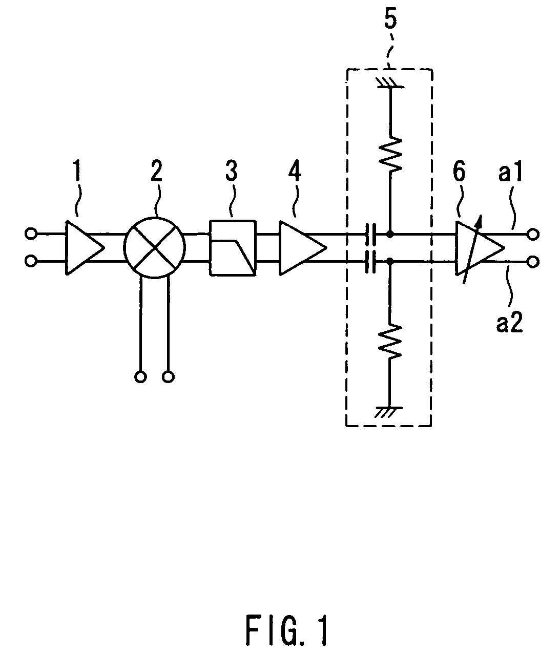
[0064]FIG. 1 shows a baseband circuit that constitutes the receiver circuit of this embodiment. The baseband circuit includes a low noise amplifier (referred to as “LNA” in the following) 1, a mixer 2, a low-pass filter 3, a fixed gain amplifier 4, a high-pass filter 5, and a gain control amplifier 6. An output of the fixed gain amplifier 4 is input to the high-pass filter 5, and an output of the high-pass filter 5 is input to the gain control amplifier 6. The gain of the fixed gain amplifier 4 is 0 dB or more. The maximum gain of the gain control amplifier 6 is 0 dB or less.

[0065]The operation of this circuit using the fixed gain amplifier 4 (with a gain of 0 dB or more) and the gain control amplifier 6 (with a maximum gain of 0 dB or less) will be described by comparison with a conventional circuit using a gain control amplifier 214, as shown in...

embodiment 2

[0083]A direct conversion receiver circuit of Embodiment 2 of the present invention will be described by referring to FIGS. 4 and 5.

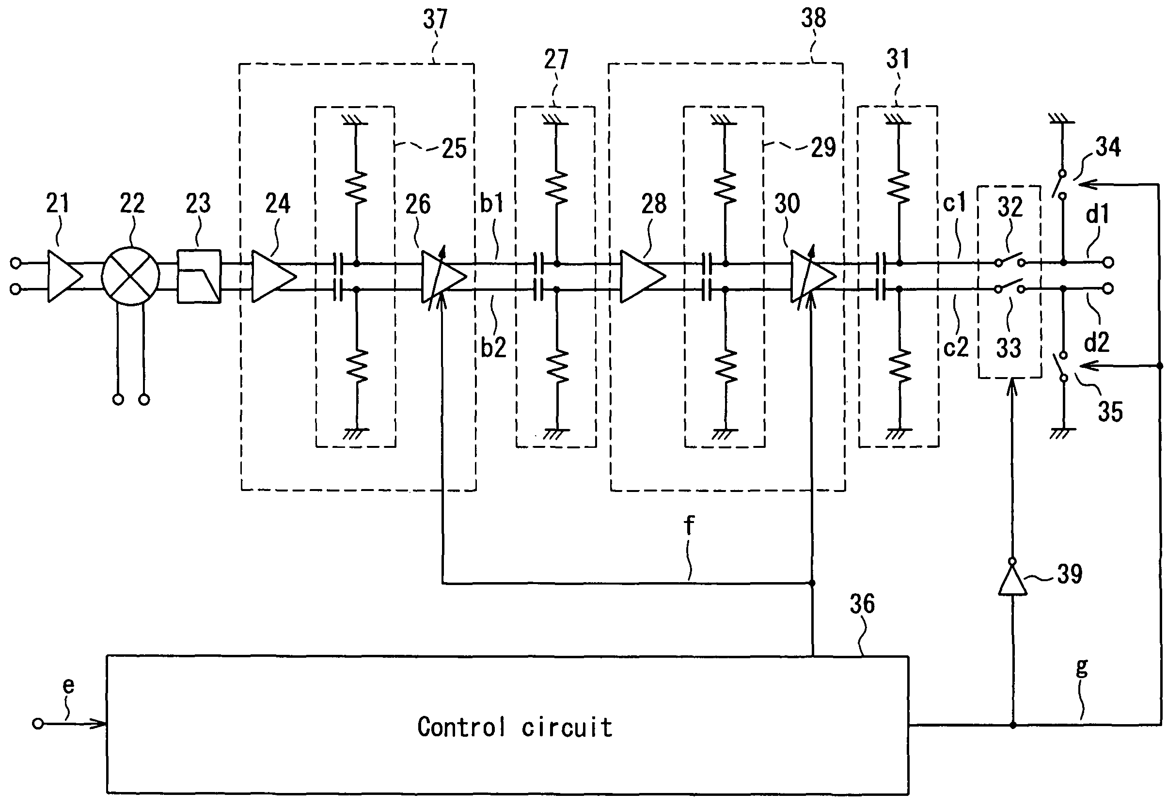
[0084]FIG. 4 shows a baseband circuit that constitutes the receiver circuit of this embodiment. The baseband circuit includes a LNA 21, a mixer 22, and a low-pass filter 23, which may be the same as those used in the circuit of Embodiment 1 as shown in FIG. 1. After the low-pass filter 23, composite amplifiers 37, 38 including fixed gain amplifiers 24, 28, high-pass filters 25, 29, and gain control amplifiers 26, 30, respectively, are connected in multiple stages. The fixed gain amplifiers 24, 28, the high-pass filters 25, 29, and the gain control amplifiers 26, 30 also may be the same as those used in the circuit of FIG. 1. The gains of the fixed gain amplifiers 24, 28 are 0 dB or more. The maximum gains of the gain control amplifiers 26, 30 are 0 dB or less. Although the circuit of FIG. 4 uses two stages of the composite amplifiers 37, 38, two or more...

embodiment 3

[0102]A direct conversion receiver circuit of Embodiment 3 of the present invention will be described by referring to FIG. 6.

[0103]FIG. 6 shows a baseband circuit that constitutes the receiver circuit of this embodiment. The baseband circuit is formed by removing the fixed gain amplifiers 24, 28 and the high-pass filter 29 from the circuit of Embodiment 2 as shown in FIG. 4. This circuit differs from the circuit of FIG. 4 in that the gains of a plurality of gain control amplifiers 301, 302 are 0 dB or more. In FIG. 6, the elements having the same functions as those in FIG. 4 are denoted by the same reference numerals.

[0104]Like the circuit of Embodiment 2, the control circuit 36 has the following functions. When a gain-change pulse is input, the control circuit 36 opens the first switches 32, 33 and closes the second switches 34, 35, and then switches the gains of the gain control amplifiers 301, 302. After a predetermined time has passed from the switching of the gains, the control...


PUM


Abstract

A receiver circuit includes a low noise amplifier (LNA) 1 to which a received signal is input, a mixer 2 for mixing an output of the LNA and a local signal, a first low-pass filter 3 for receiving an output of the mixer, and a composite amplifier in which a fixed gain amplifier 4, a high-pass filter 5, and a gain control amplifier 6 are connected in this order from the input side. An output of the first low-pass filter is input to the fixed gain amplifier. The gain of the fixed gain amplifier is 0 dB or more. The maximum gain of the gain control amplifier is 0 dB or less. The receiver circuit can suppress a transient response due to DC voltage fluctuations, even if the gains are changed while signals are received in a communication mode that performs continuous reception.

Description

FIELD OF THE INVENTION[0001]The present invention relates to a direct conversion receiver circuit.BACKGROUND OF THE INVENTION[0002]There has been a growing demand for small low-cost radio communication equipment. To meet this demand, a direct conversion receiver circuit is advantageous because the high-frequency circuit portion is simple, and the number of components can be decreased. However, the direct conversion receiver circuit also has some disadvantages, and one of the major disadvantages is a DC offset voltage.[0003]The DC offset voltage is amplified as the gain of a baseband circuit is increased. Therefore, when the gain of the baseband circuit is the maximum (e.g., 60 dB), the DC offset voltage becomes larger than the power supply voltage of the baseband circuit. Consequently, no signal is transmitted to the output of the baseband circuit.[0004]The DC offset voltage in a conventional direct conversion receiver circuit has been addressed, e.g., by JP 2003-224489 A. FIG. 20 s...

Claims


Application Information

Patent Timeline
Patent Type & Authority Patents(United States)
IPC IPC(8): H04B1/06
CPCH03D3/008
Inventor KURIMOTO, HIDEHIKO
Owner PANASONIC SEMICON SOLUTIONS CO LTD
Why Eureka
Try Eureka