Display apparatus and driving method for display apparatus

a technology of display apparatus and driving method, which is applied in the direction of instruments, static indicating devices, electroluminescent light sources, etc., can solve the problems of loss of uniformity of screen, difficulty in implementing a large-scale display apparatus having high definition, etc., and achieve the optimization of negative feedback feedback amount, uniform picture quality, and correction of mobility against dispersion

Inactive Publication Date: 2010-09-28
SONY CORP
View PDF3 Cites 7 Cited by
  • Summary
  • Abstract
  • Description
  • Claims
  • Application Information

AI Technical Summary

Benefits of technology

[0015]Therefore, it is demanded to provide a display apparatus and a driving method therefor wherein a correction function against dispersion of the mobility of a driving transistor among pixels is implemented with low power consumption to obtain a display image of uniform picture quality free from strips or luminance ununiformity.
[0017]In the display apparatus, since the drain-source current of the driving transistor is negatively fed back to the gate input side of the driving transistor, the current value of the drain-source current is uniformized among the pixels which are different in mobility. As a result, correction of the mobility against dispersion is achieved. The feedback amount in the negative feedback can be optimized by adjusting the correction time for the mobility. The optimum mobility correction time decreases as the input signal voltage increases. In other words, the optimum mobility correction time and the input signal voltage have an inverse proportional relationship to each other. Accordingly, by setting the mobility correction time in inverse proportion to the input signal voltage, the dependence of the drain-source current of the driving transistor upon the mobility can be canceled with certainty over an overall level range of the input signal voltage from the black level to the white level.
[0018]With the display apparatus, since the dependence of the drain-source current of the driving transistor upon the mobility can be canceled over an overall level range or over all gradations of the input signal voltage from the black level to the white level, a display image of uniform picture quality free from a stripe or uneven luminance arising from the fact that the mobility of the driving transistor differs among the different pixels can be obtained.

Problems solved by technology

However, although the display apparatus of the simple matrix type is simple in structure, it has such a problem that it is difficult to implement a display apparatus of a large size having high definition.
Since, if the threshold voltage Vth is different among different driving transistors, then the values of current flowing through the driving transistors exhibit dispersion, even if the same voltage is applied to the gate of the driving transistors, the organic EL elements emit light in different luminance, resulting in loss of the uniformity of the screen.

Method used


Image

  • Display apparatus and driving method for display apparatus
  • Display apparatus and driving method for display apparatus
  • Display apparatus and driving method for display apparatus

Examples


Embodiment Construction

[0041]Embodiments of the present invention will be described in detail below, referring to the drawings.

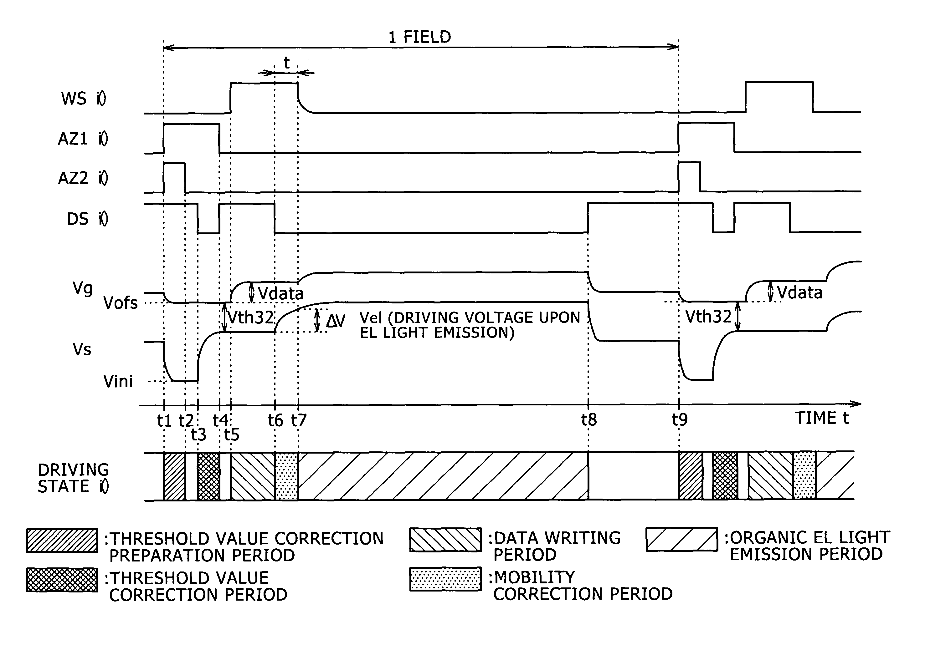
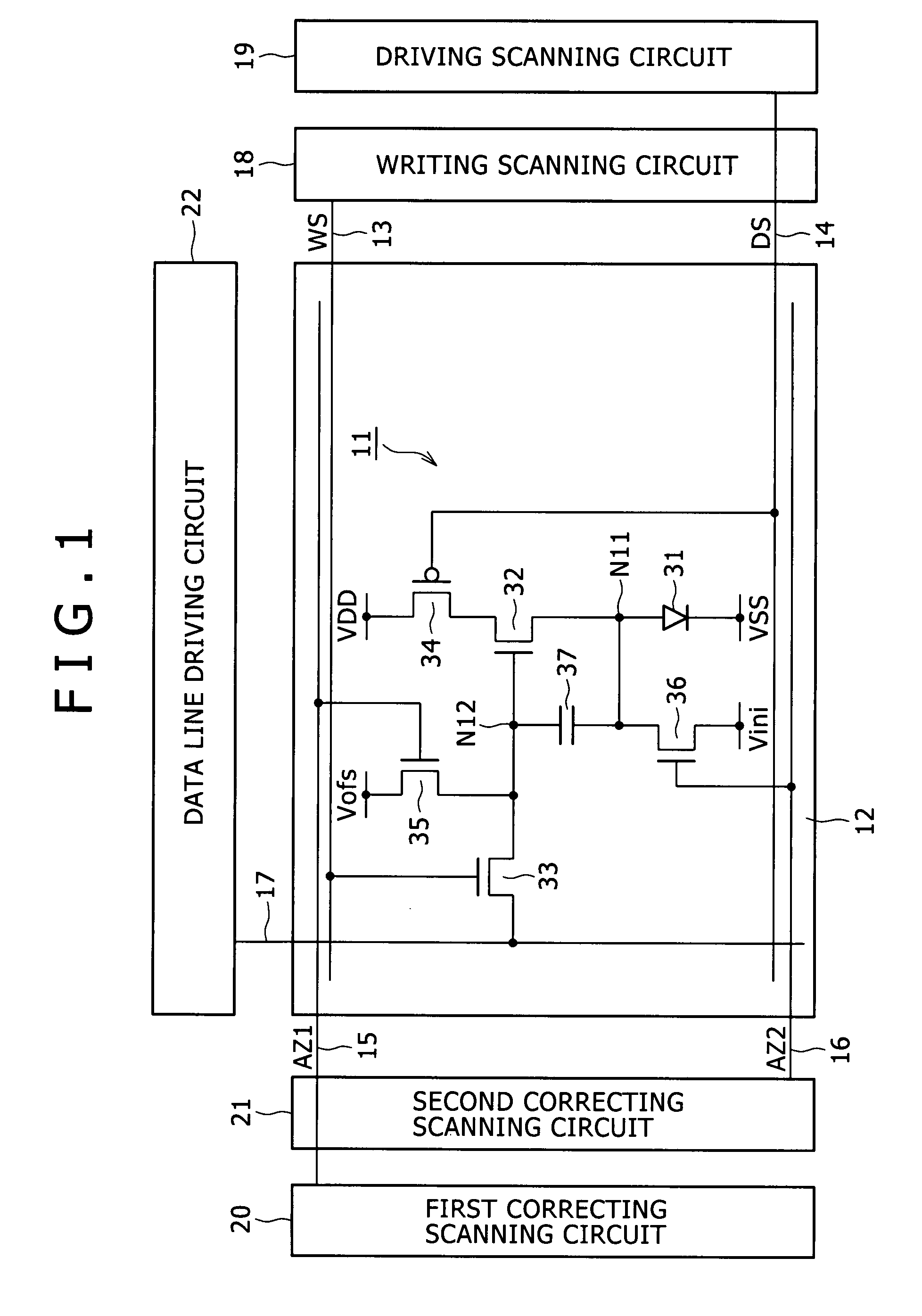
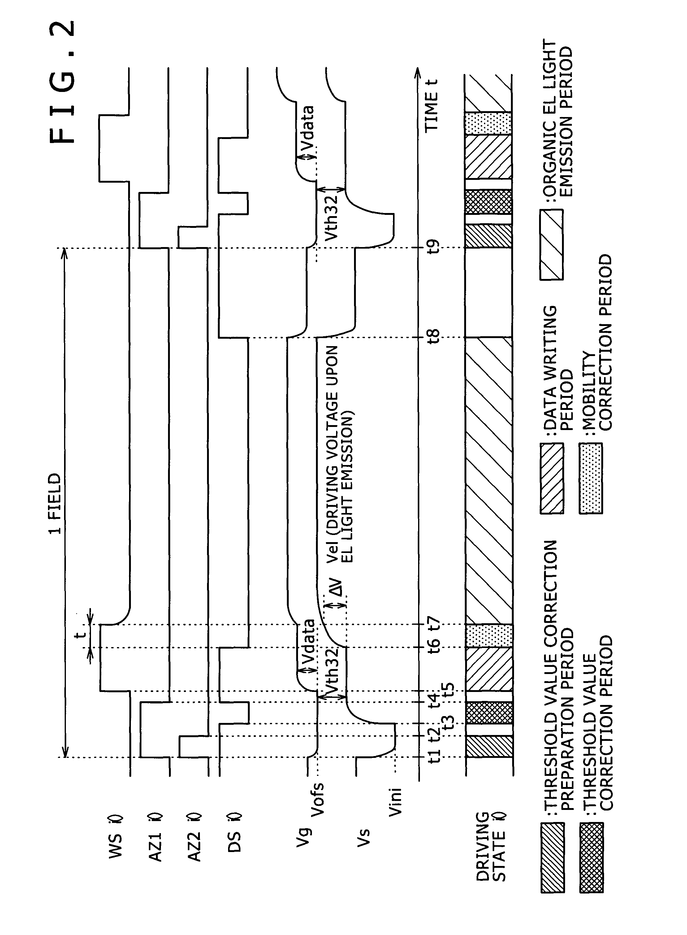
[0042]FIG. 1 shows a configuration of an active matrix display apparatus to which an embodiment of the present invention is applied and a pixel circuit used in the display apparatus.

(Pixel Array Section)

[0043]Referring to FIG. 1, the active matrix type organic EL display apparatus according to the embodiment of the present embodiment includes a pixel array section 12 wherein a plurality of pixel circuits 11 each including, as a light emitting element of a pixel, an electro-optical element of the current driven type whose light emission luminance varies in response to the value of current flowing therethrough such as, for example, an organic EL element 31 are disposed two-dimensionally in a matrix. In FIG. 1, for the simplified illustration, a particular circuit configuration of one of the pixel circuits 11 is shown.

[0044]In the pixel array section 12, for each of the pixel circuit...


PUM


Abstract

A display apparatus includes: a pixel array section and dependence cancellation means. The pixel array section wherein a plurality of pixel circuits each including an electro-optical element, a driving transistor configured to drive said electro-optical element, a sampling transistor configured to sample and write an input signal voltage and a capacitor configured to hold a gate-source voltage of said driving transistor within a display period are disposed in a matrix. The dependence cancellation means for negatively feeding back, within a correction period before said electro-optical element emits light in a state wherein the input signal voltage is written by said sampling transistor, drain-source current of said driving transistor to the gate input side of said driving transistor to cancel the dependence of the drain-source current of said driving transistor on the mobility.

Description

CROSS REFERENCES TO RELATED APPLICATIONS[0001]The present invention contains subject matter related to Japanese Patent Application JP 2006-210620 filed with the Japan Patent Office on Aug. 2, 2006, the entire contents of which being incorporated herein by reference.BACKGROUND OF THE INVENTION[0002]1. Field of the Invention[0003]This invention relates to a display apparatus and a driving method for a display apparatus, and more particularly to a display apparatus wherein a plurality of pixel circuits each including an electro-optical element are disposed in a matrix and a driving method for the display apparatus.[0004]2. Description of the Related Art[0005]In recent years, in the field of image display apparatus, an organic EL (electroluminescence) display apparatus has been developed and commercialized wherein a large number of pixel circuits each including an electro-optical element of the current driven type whose light emission luminance varies in response to the value of current...

Claims


Application Information

Patent Timeline
Patent Type & Authority Patents(United States)
IPC IPC(8): G09G3/30H05B44/00
CPCG09G3/3233G09G3/3266G09G2300/0819G09G2300/0842G09G2300/0852G09G2300/0861G09G2310/066G09G2320/043G09G2330/02G09G3/30G09G3/32G09G3/20H05B33/12
Inventor ASANO, MITSURU
Owner SONY CORP
Why Eureka
Try Eureka