Power supply device
a power supply device and power supply technology, applied in the direction of machines/engines, mechanical equipment, transportation and packaging, etc., can solve the problems of reducing the voltage drop in the dc voltage source made of batteries, requiring a large number of high-capacity power storage elements, and reducing so as to reduce the number of power storage elements necessary, reduce the number of power storage elements, and reduce the effect of the on/off ratio d
- Summary
- Abstract
- Description
- Claims
- Application Information
AI Technical Summary
Benefits of technology
Problems solved by technology
Method used
Image

Examples
first exemplary embodiment
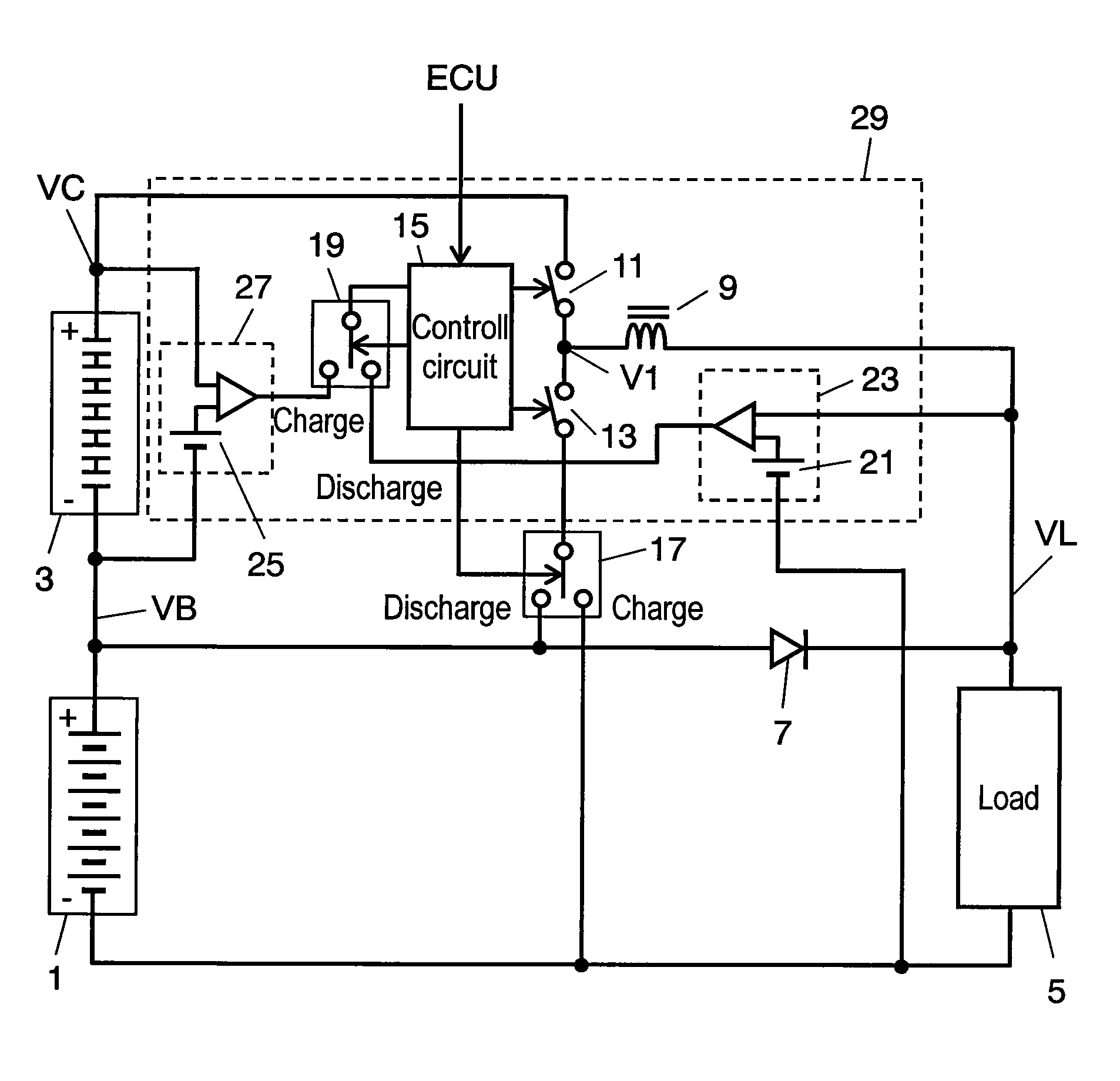
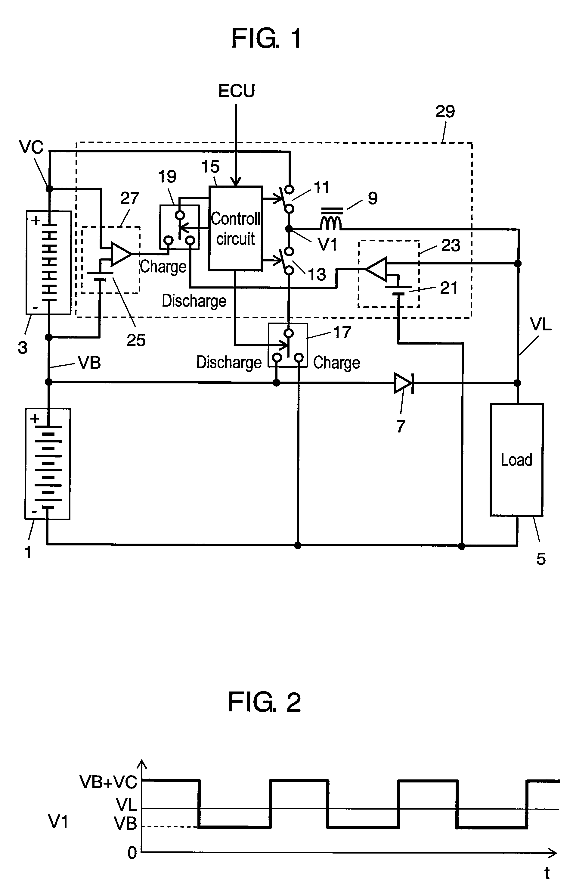
[0032]FIG. 1 is a block circuit diagram of a power supply device in accordance with the first exemplary embodiment of the present invention. FIG. 2 is a timing chart, i.e. a diagram showing a change of voltage V1 with time in the power supply device in accordance with the first exemplary embodiment of the present invention.
[0033]With reference to FIG. 1, auxiliary voltage source 3 is connected in series with DC voltage source 1 made of batteries. Used for auxiliary voltage source 3 is a power storage element made of a high-capacity electric double-layer capacitor particularly excellent in rapid charge / discharge characteristics. Load 5 that consumes power is coupled to the junction point between DC voltage source 1 and auxiliary voltage source 3, via diode 7. To one end of load 5, inductance element 9 is connected. Inductance element 9 works to smooth the power to be supplied to load 5.
[0034]First switching element 11 is connected to the other end of inductance element 9 and to one e...
second exemplary embodiment
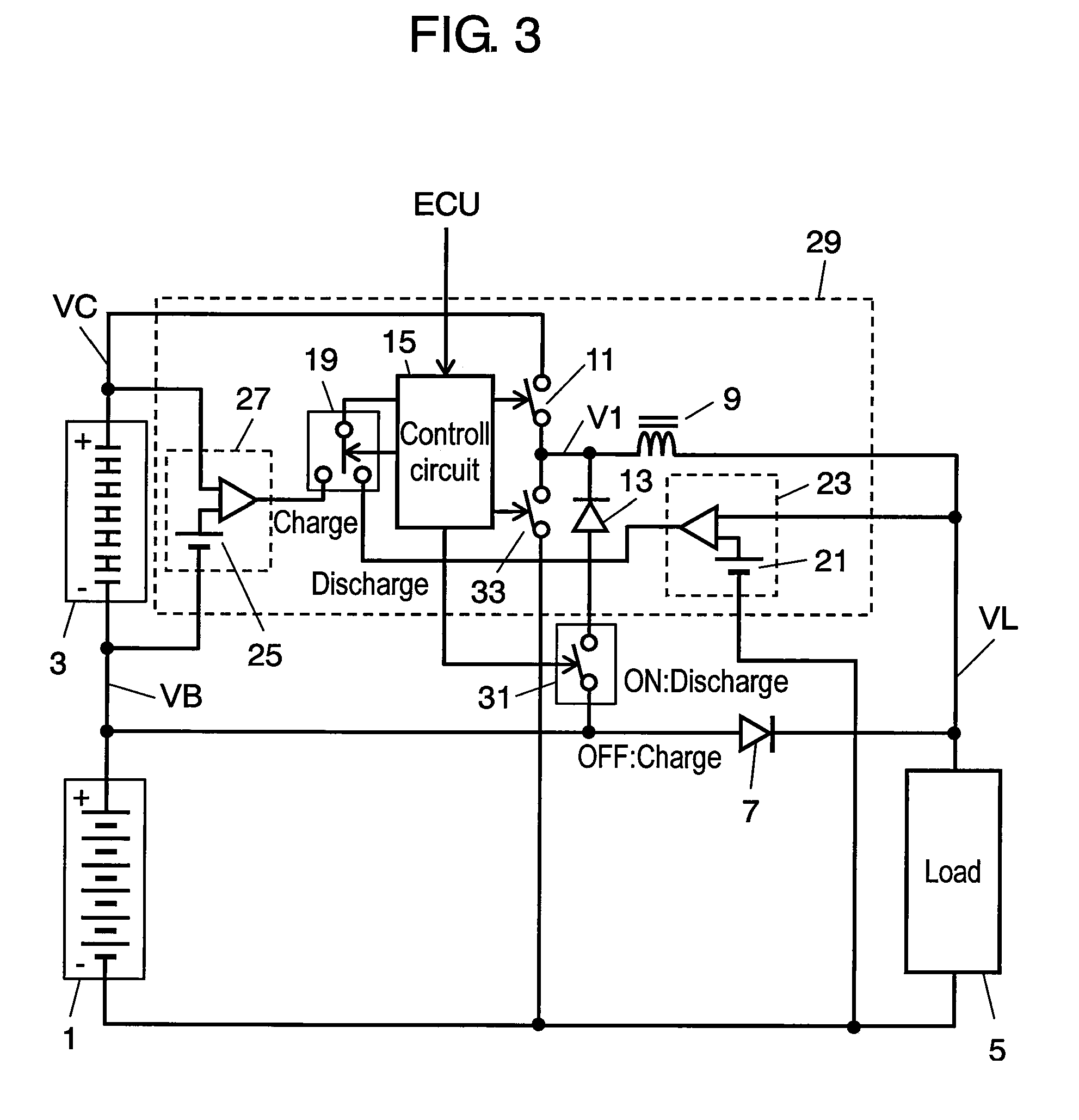
[0053]FIG. 3 is a block circuit diagram of a power supply device in accordance with the second exemplary embodiment of the present invention. In FIG. 3, elements similar to those in FIG. 1 have the same reference marks, and the detailed descriptions of these elements are omitted.
[0054]The differences in structure between FIG. 3 and FIG. 1 are listed as follows:
[0055](1) Second switching element 13 is made of a rectifier (diode). Thus, control circuit 15 controls the power to be supplied to load 5 by changing on / off ratio D2 of first switching element 11.
[0056](2) Selector switch 17 is eliminated, and switch 31 is provided so that the switch is connected in series with second switching element 13 and switched on when power is supplied to load 5. The on / off control of switch 31 is made by control circuit 15.
[0057](3) Third switching element 33 is provided so that the switching element is connected between first switching element 11 and the negative terminal of DC voltage source 1, rep...
PUM
 Abstract
Description
Claims
Application Information