Semiconductor color image sensor responsive at shorter wavelengths

a color image sensor and semiconductor technology, applied in the field of semiconductor color image sensors, can solve the problems of limited penetration depth of this shorter wavelength light at these wavelengths in silicon, short wavelength spectral response, high cost of complex fabrication, etc., and achieve the effect of improving sensitivity, enhancing image sensor performance, and better matching the maximum spectral respons

Inactive Publication Date: 2010-11-09
INTEMATIX
View PDF9 Cites 41 Cited by
  • Summary
  • Abstract
  • Description
  • Claims
  • Application Information

AI Technical Summary

Benefits of technology

[0009]The object of the invention is to provide a color image sensor which at least in part has an improved sensitivity at shorter wavelengths of the visible spectrum. Embodiments of the invention are based on converting blue light transmitted by a blue filter into longer wavelengths ranging from green to red or even near infra red (IR), for which silicon detectors have an optimum sensitivity. This is achieved through the use of a phosphor material (photo-luminescent or wavelength conversion) material to absorb shorter wavelength radiation (light) and re-emit radiation of a longer wavelength at which the sensor is more responsive. By using a phosphor material as a spectral shifter (wavelength converter) it is possible to better match the maximum spectral response (the peak of quantum efficiency) of photo-sensor and thereby greatly enhances the performance of the image sensor.
[0010]Many green, yellow, and red phosphors have been developed for the converting blue light generated by blue LEDs to white light and / or other colors, and these can be utilized in the present invention for efficiently shifting shorter wavelength light, namely blue light, to longer wavelengths before that radiation reaches the silicone detector area addressed for (or assigned to) blue part of the pixel. A variety of thin layer processing methods can be used to apply the blue light excited phosphor layer between blue filters and the blue addressed silicone detectors.
[0014]In one embodiment the image sensor further comprises a wavelength selective layer interposed between the blue filter element and the at least one phosphor material, said wavelength selective layer being substantially transparent to blue light and substantially reflective to light of said longer wavelength range. Such a filter improves the sensor sensitivity by re-directing the longer wavelength light in a direction toward the associated photo-sensor.

Problems solved by technology

Additionally, there may a limited penetration depth of this shorter wavelength light at these wavelengths in silicon.
Unfortunately, much of the radiation is absorbed at the polysilicon gate region, with very little penetrating into the channel regions of the photo-sensor where the photoelectric signal is generated.
These approaches have achieved relatively good results in terms of short wavelength spectral response, but at the high cost of complicated fabrication.
This problem has become a bottleneck to a continuing improvement of dark sensitivity and the color quality of today's digital color cameras which demand inexpensive image sensors.

Method used


Image

  • Semiconductor color image sensor responsive at shorter wavelengths
  • Semiconductor color image sensor responsive at shorter wavelengths
  • Semiconductor color image sensor responsive at shorter wavelengths

Examples


Embodiment Construction

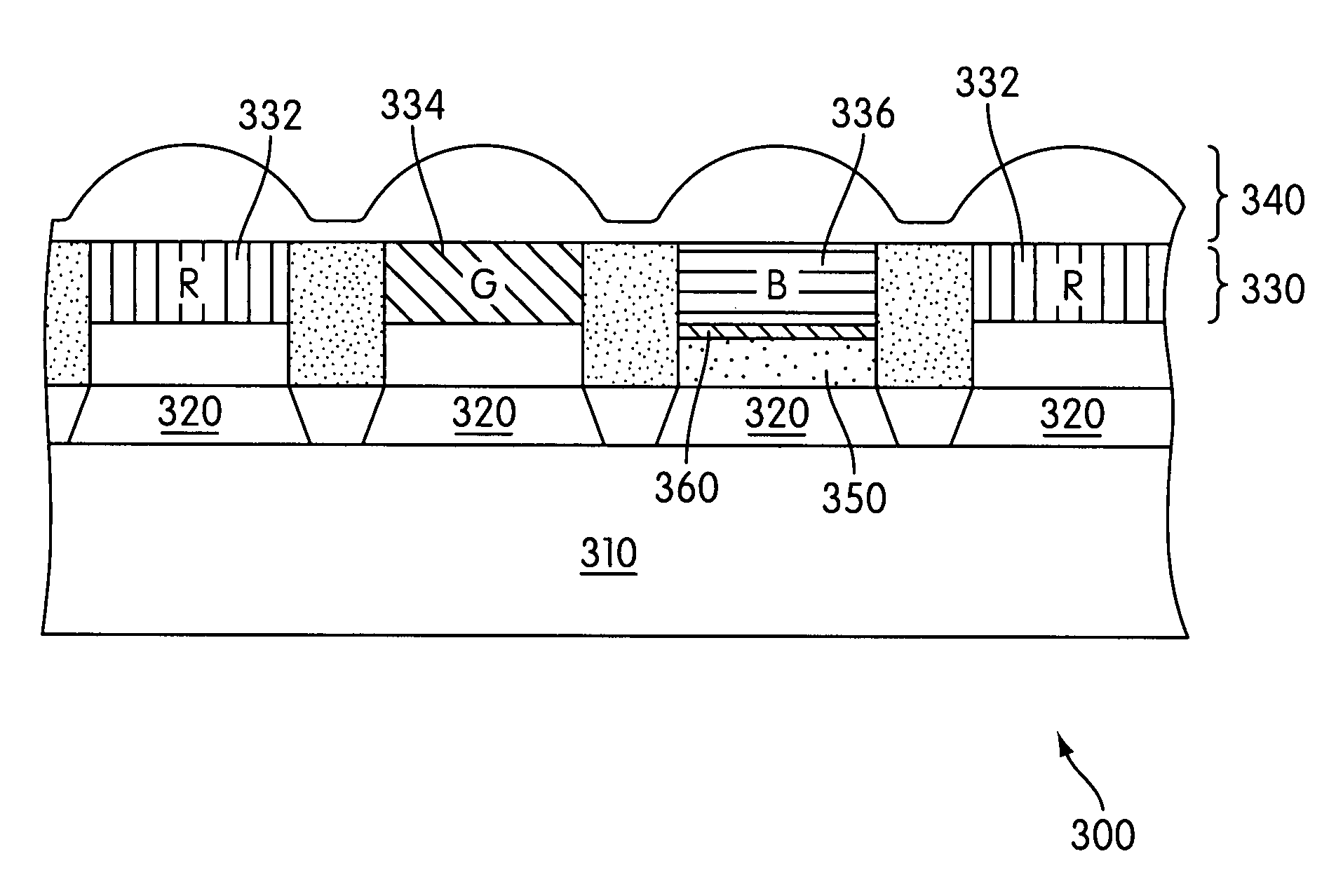
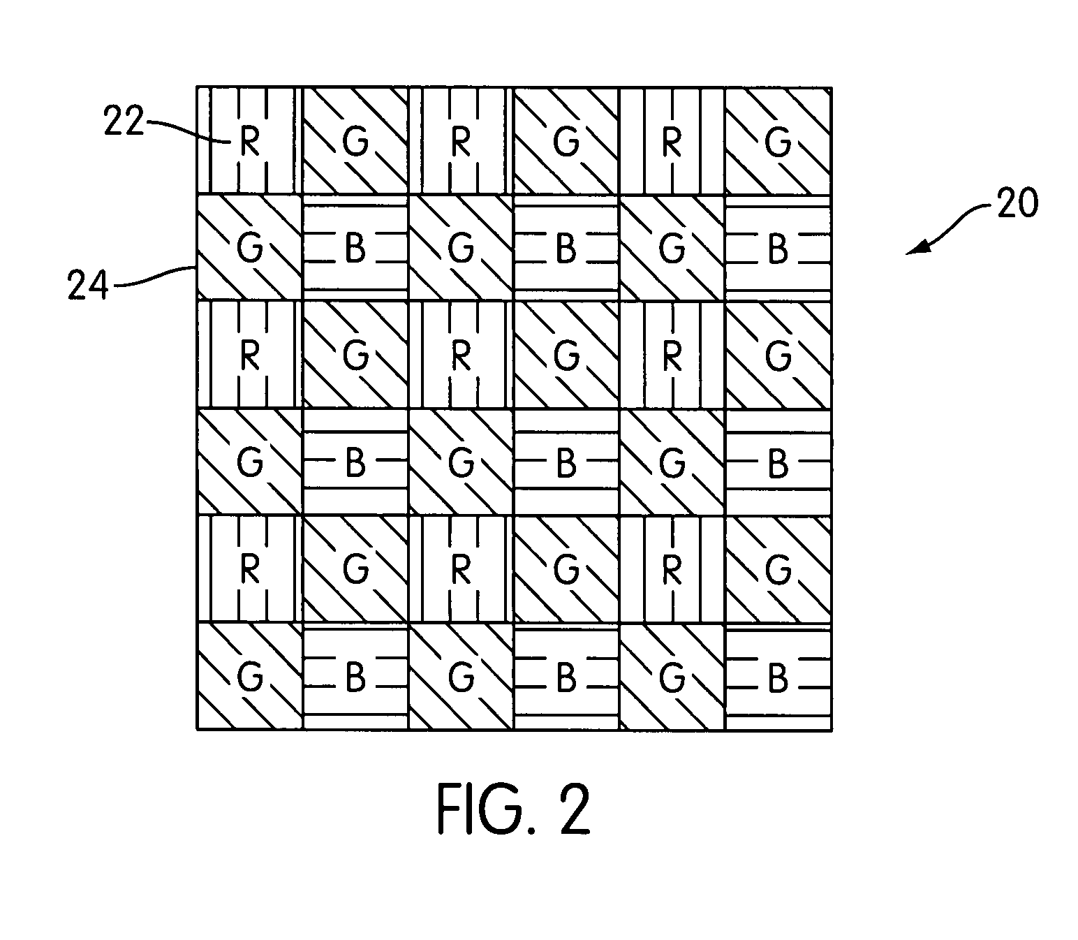
[0034]Referring to FIG. 3 there is a shown a schematic representation of a color image sensor 300 in accordance with the invention. As with the known color image sensors, the image sensor of the present invention comprises a substrate 310, typically silicon, having on an upper surface thereof an array of photo-sensors 320. The photo-sensors 320 can comprises Complementary Metal Oxide Semiconductor (CMOS) devices, Charge Coupled Devices (CCD) or other photo-detector known in the art. A color filter array (CFA) 330 is provided on top of the array of photo-sensors and comprises an array of red (R) 332, green (G) 334 and blue (B) 336 filter elements. As is known the CFA 330 is configured such that a respective filter element overlies an associated photo-sensor 320. The CFA can comprise a Bayer mosaic pattern of red, green and blue filter elements in which there are twice as many green filter elements as there are red and blue filter elements as for example illustrated in FIG. 2. Each fi...


PUM

PropertyMeasurementUnit
wavelengthaaaaaaaaaa
wavelength rangeaaaaaaaaaa

Abstract

A semiconductor color image sensor comprises: an array of semiconductor photo-sensors (CMOS or CCD) and a color filter array comprising an array of red, green and blue filter elements in which each filter element is associated with a respective one of the photo-sensors. The sensor further comprises a phosphor (photo-luminescent) material associated with each of the blue filter elements and configured to absorb blue light and re-emit light of a longer wavelength range which is then incident on the photo-sensor associated with the blue filter element. Preferably the phosphor material is selected such that light of the longer wavelength range substantially matches the spectral response of the photo-sensor. The image sensor can further comprise an array of micro-lenses for focusing light onto the photo-sensors of the image sensor, wherein each micro-lens is associated with a respective one of the photo-sensors.

Description

CROSS REFERENCE TO RELATED APPLICATION[0001]This application claims the benefit of priority to U.S. Provisional Patent Application No. 60 / 838,484, filed Aug. 16, 2006, the specification and drawings of which are incorporated herein by reference.BACKGROUND OF THE INVENTION[0002]1. Field of the Invention[0003]The present invention relates to semiconductor color image sensors such as CCD (Charge Coupled Devices) and CMOS (Complementary Metal Oxide Semiconductor) image sensors. In particular the invention concerns improvements in or relating to the response of such sensors at shorter wavelengths.[0004]2. Description of the Related Art[0005]As is known semiconductor image sensors comprise an array of semiconductor photo-sensors which measure the intensity of light incident on them. In a color image sensor the contribution of red (R), green (G) and blue (B) light components are measured for each pixel of the image using a color filter array (CFA) which comprises an array of red, green and...

Claims


Application Information

Patent Timeline
Patent Type & Authority Patents(United States)
IPC IPC(8): H04N5/335G01N23/04
CPCH01L27/14621H04N9/045H01L27/14627H04N25/134
Inventor LI, YI-QUNCHENG, SHIFANRYDE, MAGNUSKO, MIKE
Owner INTEMATIX
Why Eureka
Try Eureka