

Multi-stage linear voltage regulator with frequency compensation
- Summary
- Abstract
- Description
- Claims
- Application Information
AI Technical Summary
Benefits of technology
Problems solved by technology
Method used
Image

Examples
Embodiment Construction
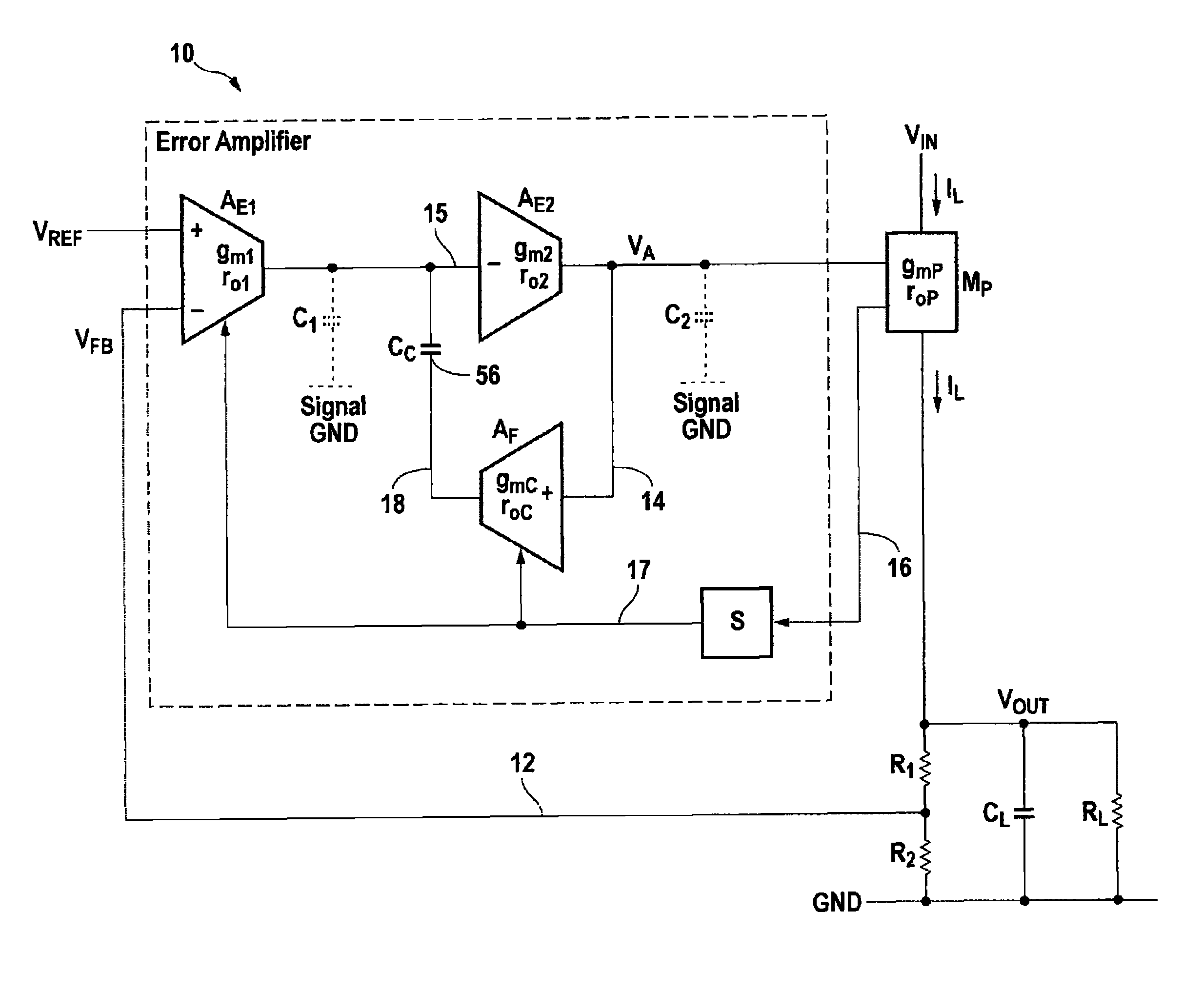
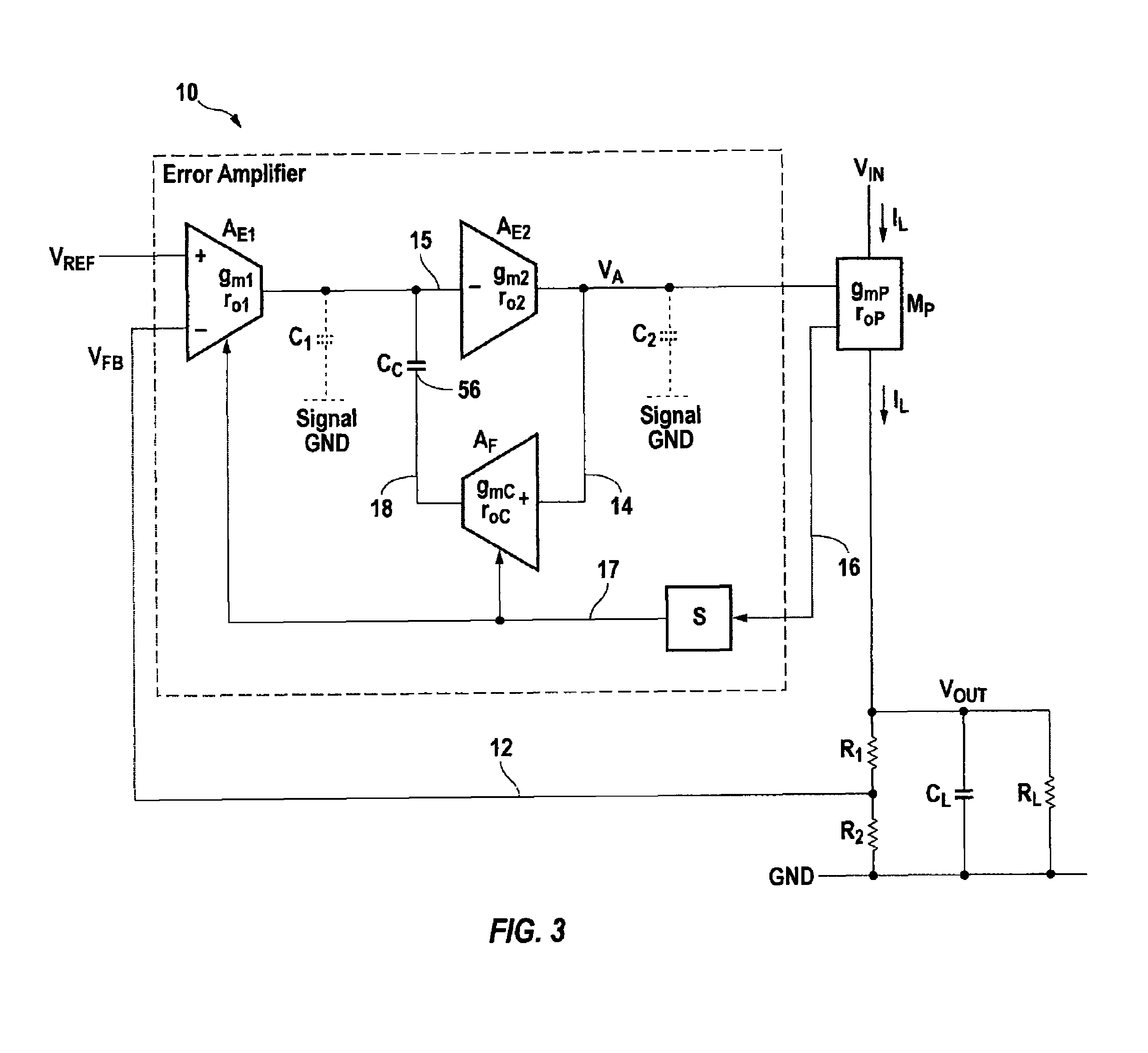
[0019]FIG. 3 is an illustration of a specific embodiment of a two-gain-stage linear voltage regulator with error amplifier 10 with frequency compensation according to the invention. The object is to cause VOUT to track VREF over a wide loading range. The error amplifier 10 has first and second independent gain stages represented with AE1 and AE2. The transconductance and output resistance of the first stage are denoted by gm1 and ro1, respectively. The transconductance and output resistance of the second stage are denoted by gm2 and ro2, respectively. C1 and C2 are the parasitic capacitances at the output nodes of the first gain stage and second gain stage AE1 and AE2, respectively. The general LDO feedback loop 12 (aka regulation feedback path) is closed after dividing VOUT between R1 and R2 as in the prior art (FIG. 1 and FIG. 2), but this is not a necessity; it is quite possible to omit these two resistors, and feed VOUT directly back to the input of the error amplifier to equate...
PUM
 Abstract
Description
Claims
Application Information