Device and method for optical nanoindentation measurement

a technology of optical nanoindentation and measurement device, which is applied in the direction of measurement device, material hardness investigation, instruments, etc., can solve the problems of inability to measure the density of traditional nanoindentation measurement system, inability to obtain young's modulus accuracy, and inability to measure mechanical properties of thin films. achieve the effect of improving the young's modulus accuracy, facilitating a wider application of nanoindentation measurement system, and enhancing both the accuracy and the capacity of curren

Active Publication Date: 2010-12-07
IND TECH RES INST
View PDF3 Cites 4 Cited by
  • Summary
  • Abstract
  • Description
  • Claims
  • Application Information

AI Technical Summary

Benefits of technology

[0019]In short, the present invention not only improves the accuracy of the Young's modulus of the thin film measured by traditional nanoindentation measurement systems, but also makes possible the measurement of the Poisson's ratio and the density of the thin film otherwise unobtainable through traditional nanoindentation measurement systems. Technically, the present invention is able to enhance both the accuracy and the capacity of current nanoindentation measurement systems, and facilitates a wider application of the nanoindentation measurement system in terms of industry effect.

Problems solved by technology

The thickness of thin film is so thin that it distinguishes itself from bulk materials in terms of mechanical properties, and so much so that traditional experimental design has been rendered inadequate to measure the mechanical properties of thin film.
Nevertheless, if the estimation of the Poisson's ratio is significantly different from the reality, the accuracy of the obtained Young's modulus will be compromised, too.
In addition, traditional nanoindentation measurement systems are unable to measure the density, another important mechanical property, of the thin film as well.

Method used


Image

  • Device and method for optical nanoindentation measurement
  • Device and method for optical nanoindentation measurement
  • Device and method for optical nanoindentation measurement

Examples


Embodiment Construction

[0026]With detailed description of the embodiments of the present invention, those skilled in the art will readily appreciate that various modifications and changes can be applied to the embodiments of the invention as hereinbefore described without departing from its scope, defined in and by the appended claims. In addition, the embodiments should not be construed as a limitation on the implementation of applicable description of the invention.

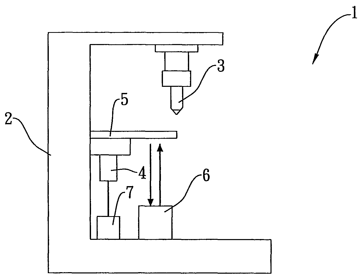
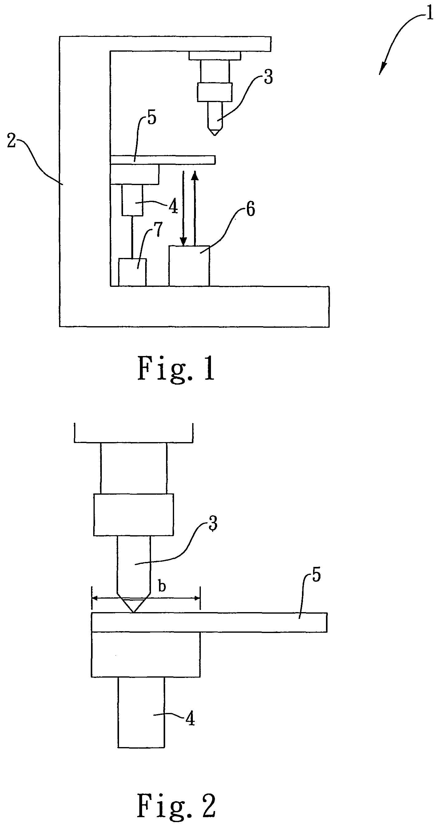
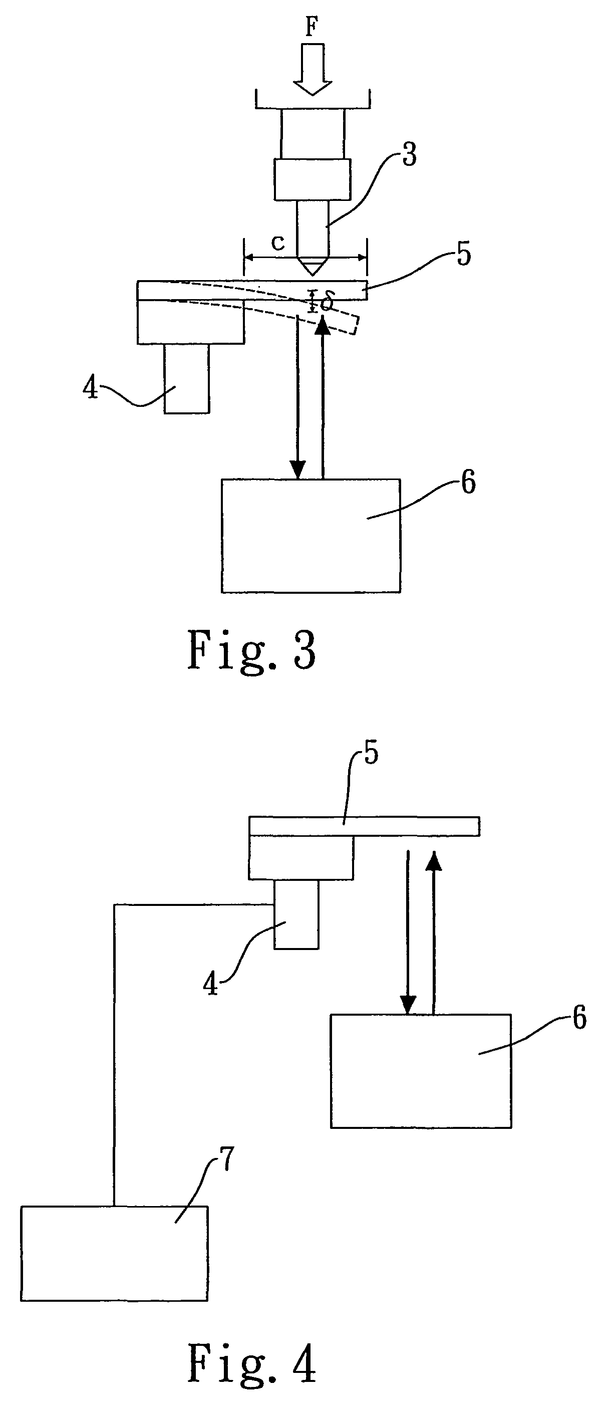
[0027]FIG. 1 shows a schematic view of a device for optical nanoindentation measurement 1 according to the present invention. The device for optical nanoindentation measurement 1 comprises a measuring station 2, an indenter tip 3, a vibrating component 4, thin film 5, and an optical transceiver 6. The indenter tip 3 is mounted on the measuring station 2, capable of moving along the measuring station 2. The vibrating component 4 is mounted on the measuring station 2 for causing the thin film 5 to vibrate. The thin film 5 is placed upon the vib...


PUM

PropertyMeasurementUnit
optical nanoindentationaaaaaaaaaa
displacementaaaaaaaaaa
frequenciesaaaaaaaaaa

Abstract

This invention relates to a device and method for optical nanoindentation measurement, according to which respective measurement results are obtained by having an indenter tip apply load to a fixed portion of a thin film, having an indenter tip apply load to a non-fixed portion of a thin film, and having a vibrating component transmit the dynamic properties of the vibration to the thin film. By combining the above measurement results in calculations, the Young's modulus, the Poisson's ratio, and the density of the thin film can be obtained.

Description

BACKGROUND OF THE INVENTION[0001]1. Field of the Invention[0002]The present invention relates to a device and method for measurement, especially a device and method for optical nanoindentation measurement.[0003]2. Description of the Related Art[0004]The wide application of thin film in the semiconductor, micro-mechanical, solar energy, and display industries over the past few years has made the mechanical properties of thin film an influencing element in deciding the performance and the service life of product. The thickness of thin film is so thin that it distinguishes itself from bulk materials in terms of mechanical properties, and so much so that traditional experimental design has been rendered inadequate to measure the mechanical properties of thin film. To tackle the problem, a variety of methods, such as bulge test, nanoindentation test, and micro tensile test, etc., have been developed in attempts to measure the mechanical properties of thin film. Nanoindentation test, in p...

Claims


Application Information

Patent Timeline
Patent Type & Authority Patents(United States)
IPC IPC(8): G01N3/48
CPCG01N3/405B82Y35/00G01Q60/366G01N2203/0286G01N2203/0641
Inventor HSU, JIONG-SHIUNLU, HUI-CHINGWU, CHUNG-LINCHEN, SHENG-JUI
Owner IND TECH RES INST
Why Eureka
Try Eureka