Manufacturing method of semiconductor device

a manufacturing method and semiconductor technology, applied in the field of semiconductor devices, can solve problems such as increasing steps and character defects, and achieve the effects of reducing writing voltage and erasing voltage, simplifying manufacturing process, and reducing characteristic defects of transistors

Inactive Publication Date: 2010-12-14
SEMICON ENERGY LAB CO LTD
View PDF16 Cites 29 Cited by
  • Summary
  • Abstract
  • Description
  • Claims
  • Application Information

AI Technical Summary

Benefits of technology

[0008]In view of the foregoing problems, it is an object of the invention to simplify the process even when a memory transistor and a transistor which has a gate insulating film with a thickness different from that in the memory transistor are formed over the same substrate. It is another object of the invention to suppress characteristic defects even when a memory transistor and a transistor which has a gate insulating film with a thickness different from that in the memory transistor are formed over the same substrate. It is a still further object of the invention to suppress characteristic defects and reduce a writing voltage and an erasing voltage even when a memory transistor and a transistor which has a gate insulating film with a thickness different from that in the memory transistor are formed over the same substrate.
[0015]A memory transistor is formed over the same substrate as a plurality of thin film transistors that have gate insulating films with different thicknesses in the invention. Furthermore, the memory transistor and some of the plurality of thin film transistors are provided to have a bottom gate structure while the other thin film transistors are provided to have a top gate structure. As a result, simplification of a manufacturing process is achieved.
[0016]The invention also includes a structure in which a memory transistor is formed over the same substrate as a plurality of thin film transistors that have gate insulating films with different thicknesses. Moreover, the thin film transistors have either a top gate structure or a bottom gate structure depending on the thicknesses of gate insulating films. Accordingly, an etching step to remove an insulating film formed in contact with a semiconductor film can be omitted, thereby reducing characteristic defects of the transistors.
[0017]A memory transistor has a bottom gate structure and electrons are injected or released into / from a charge accumulation layer by utilizing an edge of a gate electrode. As a result, a writing voltage and an erasing voltage can be reduced.

Problems solved by technology

When an unnecessary insulating film formed over a semiconductor film is removed by etching in order to separately form insulating films, the surface of the semiconductor film may be damaged by etching, leading to characteristic defects.
There is also a problem of increase in steps with the removal of an unnecessary insulating film.

Method used


Image

  • Manufacturing method of semiconductor device
  • Manufacturing method of semiconductor device
  • Manufacturing method of semiconductor device

Examples


embodiment mode 1

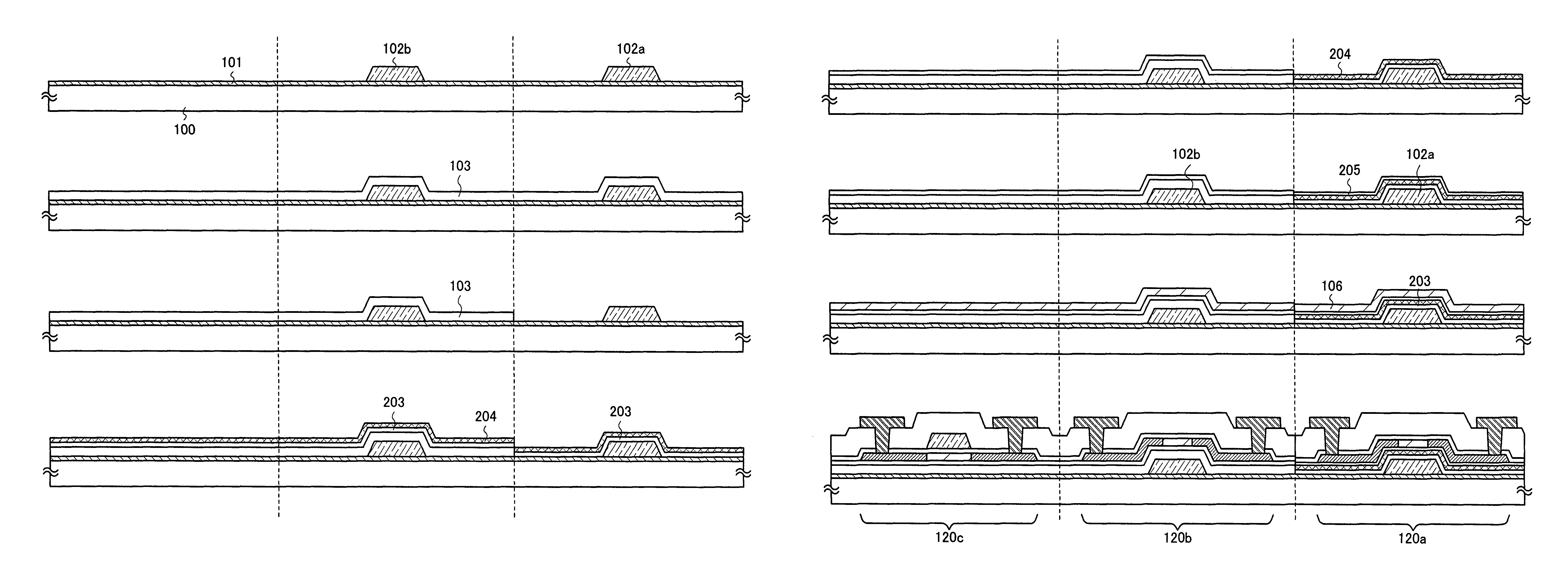
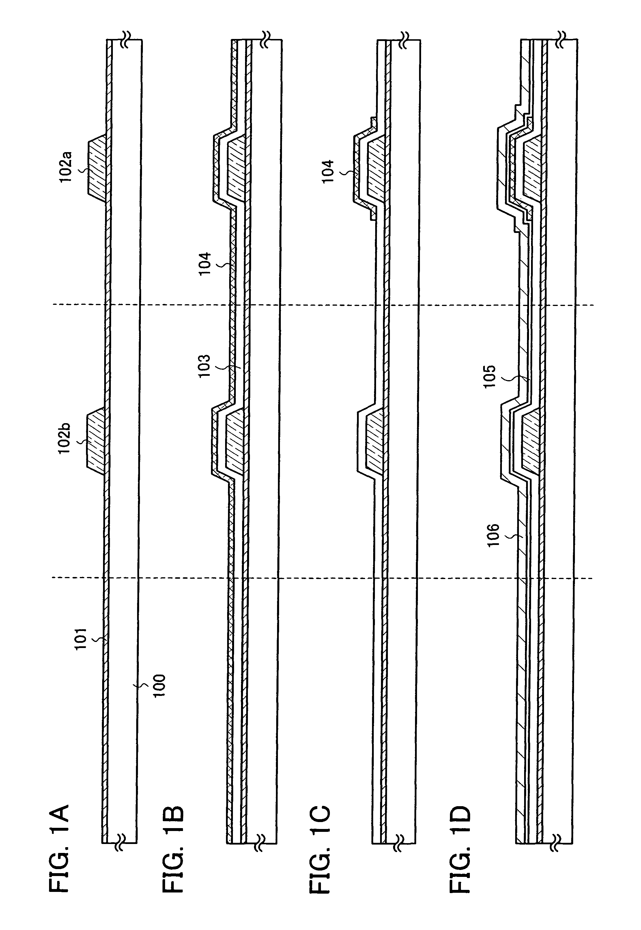
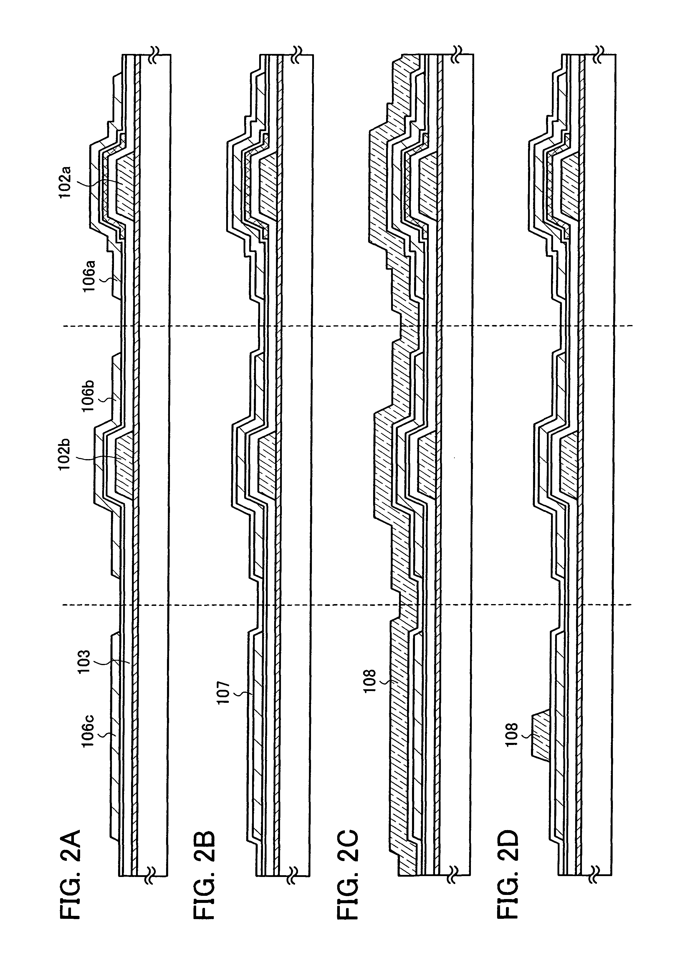
[0035]In this embodiment mode, an example of a semiconductor device including a memory transistor and a method for manufacturing the semiconductor device is described with reference to FIGS. 1A to 1D, FIGS. 2A to 2D, and FIGS. 3A to 3C.

[0036]Described hereinafter is a case in which a memory transistor is formed over the same substrate as a thin film transistor that is required to have high withstand voltage (high-voltage thin film transistor) and a thin film transistor that is required to operate at high speed (high-speed thin film transistor). A gate insulating film of the high-voltage thin film transistor is formed to have a thickness greater than that of a gate insulating film of the high-speed thin film transistor.

[0037]First, conductive films 102a and 102b are formed over a substrate 100 with an insulating film 101 interposed therebetween (see FIG. 1A).

[0038]The substrate 100 may be a glass substrate, a metal substrate, a stainless steel substrate, a plastic substrate having he...

embodiment mode 2

[0075]In this embodiment mode, a semiconductor device and a manufacturing method thereof, which are different from those shown in the above embodiment mode, are described with reference to the drawings. Specifically, a MONOS memory transistor is described, in which an insulating film (insulating film between a gate electrode and a charge accumulation layer) of a memory transistor has a thickness smaller than that of a gate insulating film of a high-voltage thin film transistor.

[0076]First, the conductive films 102a and 102b are formed over the substrate 100 with the insulating film 101 interposed therebetween (see FIG. 4A). The conductive film 102a functions as the gate electrode of the memory transistor while the conductive film 102b functions as the gate electrode of the high-voltage thin film transistor.

[0077]Then, the first insulating film 103 is formed over the substrate 100 and the conductive films 102a and 102b (see FIG. 4B). In this embodiment mode, the first insulating film...

embodiment mode 3

[0097]In this embodiment mode, a structure of a semiconductor device, which is different from that shown in the above embodiment modes, is described with reference to the drawings. Specifically, description is made on a structure in which a memory transistor and a high-voltage thin film transistor are each provided with an upper gate electrode.

[0098]The semiconductor device shown in this embodiment mode has a structure in which a conductive film 208 functioning as an upper electrode is added to the bottom gate memory transistor 120a and high-voltage thin film transistor 120b in the semiconductor device shown in FIGS. 3A to 3C (see FIG. 6A).

[0099]The conductive film 208 allows the threshold value to be controlled; thus high speed operation or low power consumption can be selected arbitrarily.

[0100]Note that the conductive film 208 functioning as an upper electrode may be added to the memory transistor 120a and the high-voltage thin film transistor 120b in the structure shown in Embod...


PUM


Abstract

The invention provides a semiconductor device and its manufacturing method in which a memory transistor and a plurality of thin film transistors that have gate insulating films with different thicknesses are fabricated over a substrate. The invention is characterized by the structural difference between the memory transistor and the plurality of thin film transistors. Specifically, the memory transistor and some of the plurality of thin film transistors are provided to have a bottom gate structure while the other thin film transistors are provided to have a top gate structure, which enables the reduction of characteristic defects of the transistor and simplification of its manufacturing process.

Description

TECHNICAL FIELD[0001]The present invention relates to a semiconductor device and a manufacturing method thereof. In particular, the invention relates to a semiconductor device including a semiconductor memory element and a manufacturing method thereof.BACKGROUND ART[0002]In recent years, multifunctional and high-performance small semiconductor devices have been rapidly developed, which are typified by mobile devices such as a mobile computer and a mobile phone. With the development of these semiconductor devices, a transistor-type semiconductor memory element (hereinafter also referred to as a “memory transistor”) has attracted attention as a memory included in the semiconductor devices.[0003]As one of the semiconductor memory elements, the market of nonvolatile memories has been growing, to which data can be electrically rewritten and stored after the power supply is shut off. The nonvolatile memories have a structure similar to MOS transistors and are characterized in that a regio...

Claims


Application Information

Patent Timeline
Patent Type & Authority Patents(United States)
IPC IPC(8): H01L21/00
CPCH01L27/105H01L27/11526H01L27/11546H01L27/11568H01L27/1214H01L27/1157H01L27/13H01L29/4234H01L29/792H01L29/7923H01L27/1251H10B41/49H10B41/40H10B43/30H10B43/35
Inventor TAKANO, TAMAEKAKEHATA, TETSUYAYAMAZAKI, SHUNPEI
Owner SEMICON ENERGY LAB CO LTD
Why Eureka
Try Eureka