

Liquid crystal display device which reduces unevenness in an upper surface of at least an electrode
a liquid crystal display device and upper surface technology, applied in non-linear optics, instruments, optics, etc., can solve the problems of reducing contrast, misalignment of liquid crystal molecules, and achieving the effect of reducing contrast caused by concavity and convexities of electrodes on the main surface (inner surface) of the substrate, ensuring sufficient light transmi
- Summary
- Abstract
- Description
- Claims
- Application Information
AI Technical Summary
Benefits of technology
Problems solved by technology
Method used
Image

Examples
first embodiment
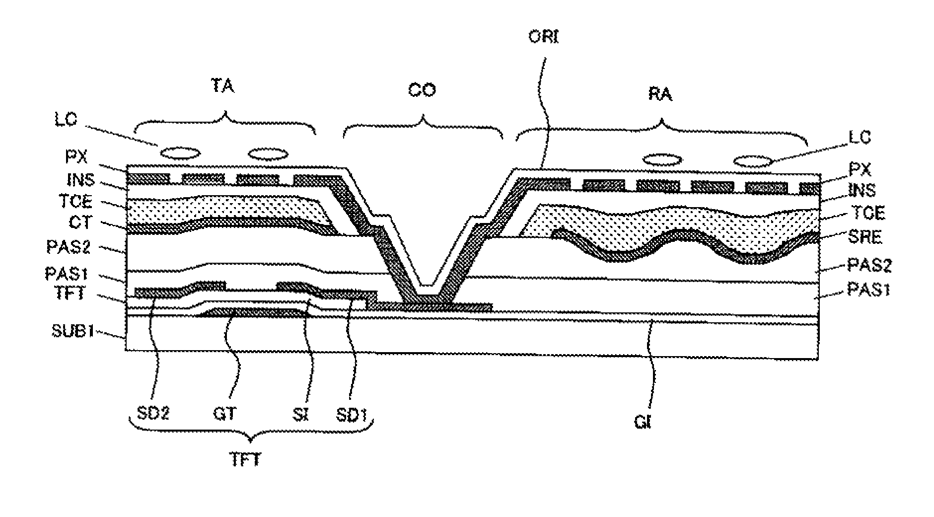
[0041]FIG. 1 is a partial cross-sectional view of a semi-transmissive liquid crystal display device having both a transmissive display part and a reflective display part, illustrating the first embodiment of the present invention. In FIG. 1, a thin film transistor TFT is formed on the main surface of a glass substrate SUB1 as an insulating substrate. The thin film transistor TFT is composed of a gate electrode GT, a gate insulating film GI, a silicon semiconductor layer SI, a drain electrode SD1, and a source electrode SD2.
[0042]An inorganic insulating film PAS1 and an organic insulating film PAS2 are sequentially formed to cover the thin film transistor TFT, and a base electrode CT is formed on these inorganic and organic insulating films. The base electrode CT is a pixel electrode in a transmissive display part TA and is a scattering reflective electrode SRE in a reflective display part RA. The base electrode CT of the transmissive display part TA has concavities and convexities t...
second embodiment
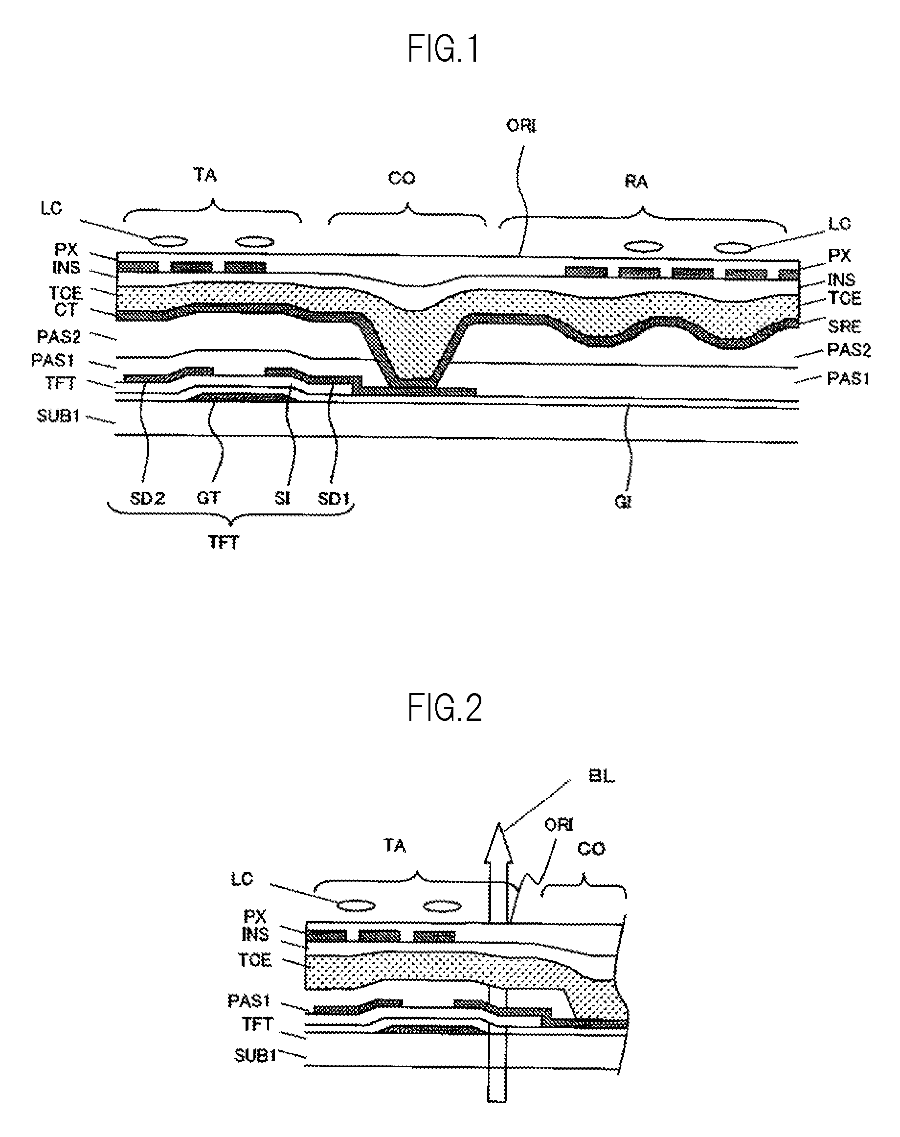
[0047]FIG. 2 is a partial cross-sectional view of the transmissive display part TA of a semi-transmissive liquid crystal display device having both a transmissive display part and a reflective display part, illustrating the second embodiment of the present invention. In FIG. 2, the same reference numerals as FIG. 1 show the same functional portions. In the second embodiment, the base electrode CT and the organic insulating film PAS2 in FIG. 1 have been removed. In other words, the first electrode TCE is disposed directly on the inorganic insulating film PAS1, and the result is used as a pixel electrode (or a common electrode). The structure of the reflective display part RA is also the same. The base electrode CT (including the scattering reflective electrode SRE) and the organic insulating film PAS2 are removed, the first electrode TCE is directly disposed on the inorganic insulating film PAS1, and this is used as a scattering reflective electrode. Accordingly, the structure can be...
PUM
| Property | Measurement | Unit |
|---|---|---|
| total light transmittance | aaaaa | aaaaa |
| light transmittance | aaaaa | aaaaa |
| surface flatness | aaaaa | aaaaa |
Abstract
Description
Claims
Application Information