ESD device layout for effectively reducing internal circuit area and avoiding ESD and breakdown damage and effectively protecting high voltage IC

a technology of esd device and internal circuit, applied in emergency protective circuit arrangements, transistors, etc., can solve the problems of static electricity and electrostatic discharge, semiconductor devices no longer function or be partially degraded, premature failure, etc., to reduce chip area, curtail esd reliability issue, and improve esd protection capability

Inactive Publication Date: 2010-12-21
HIMAX TECH LTD
View PDF6 Cites 0 Cited by
  • Summary
  • Abstract
  • Description
  • Claims
  • Application Information

AI Technical Summary

Benefits of technology

[0012]By properly adjusting the breakdown voltage of I / O circuit, i.e. adjusting the distance between a well of a conductivity type and a heavily doped region according to the proposed method, it will help to reduce the chip area as well as curtailing the ESD reliability issue. The present invention will improve a product's ESD durability.

Problems solved by technology

Static electricity has been an industrial problem for centuries.
The age of electronics brought with it new problems associated with static electricity and electrostatic discharge (“ESD”).
The ESD damage may be either a catastrophic failure or a latent defect which may cause the semiconductor device no longer function or be partially degraded and experience premature failure.
It will increase the associated costs for repair, replacement, and et al.
The outermost ESD circuit device within an input / output circuit (“I / O”) will induce ESD disaster if the ESD circuit device follows the same conventional layout rules.
It may not be able to safeguard the whole chip against ESD because the breakdown voltage of internal circuit will be lower than the breakdown voltage of I / O circuit.
On the other hand, if the ESD circuit device follows that same layout rules as internal circuit, it will affect the durability of the ESD circuit when the IC is not connected to the circuit board and / or power-off and / or floating.
As a result, the ESD device within I / O circuit will not be able to function properly to protect the internal circuit from power noise damage.
The problem causes the p-n well junction breakdown voltage of internal circuit to be lower than the p-n well junction breakdown voltage of I / O circuit.
Hence, the internal circuit will suffer from the damage of abrupt voltage pulse.

Method used


Image

  • ESD device layout for effectively reducing internal circuit area and avoiding ESD and breakdown damage and effectively protecting high voltage IC
  • ESD device layout for effectively reducing internal circuit area and avoiding ESD and breakdown damage and effectively protecting high voltage IC
  • ESD device layout for effectively reducing internal circuit area and avoiding ESD and breakdown damage and effectively protecting high voltage IC

Examples


first embodiment

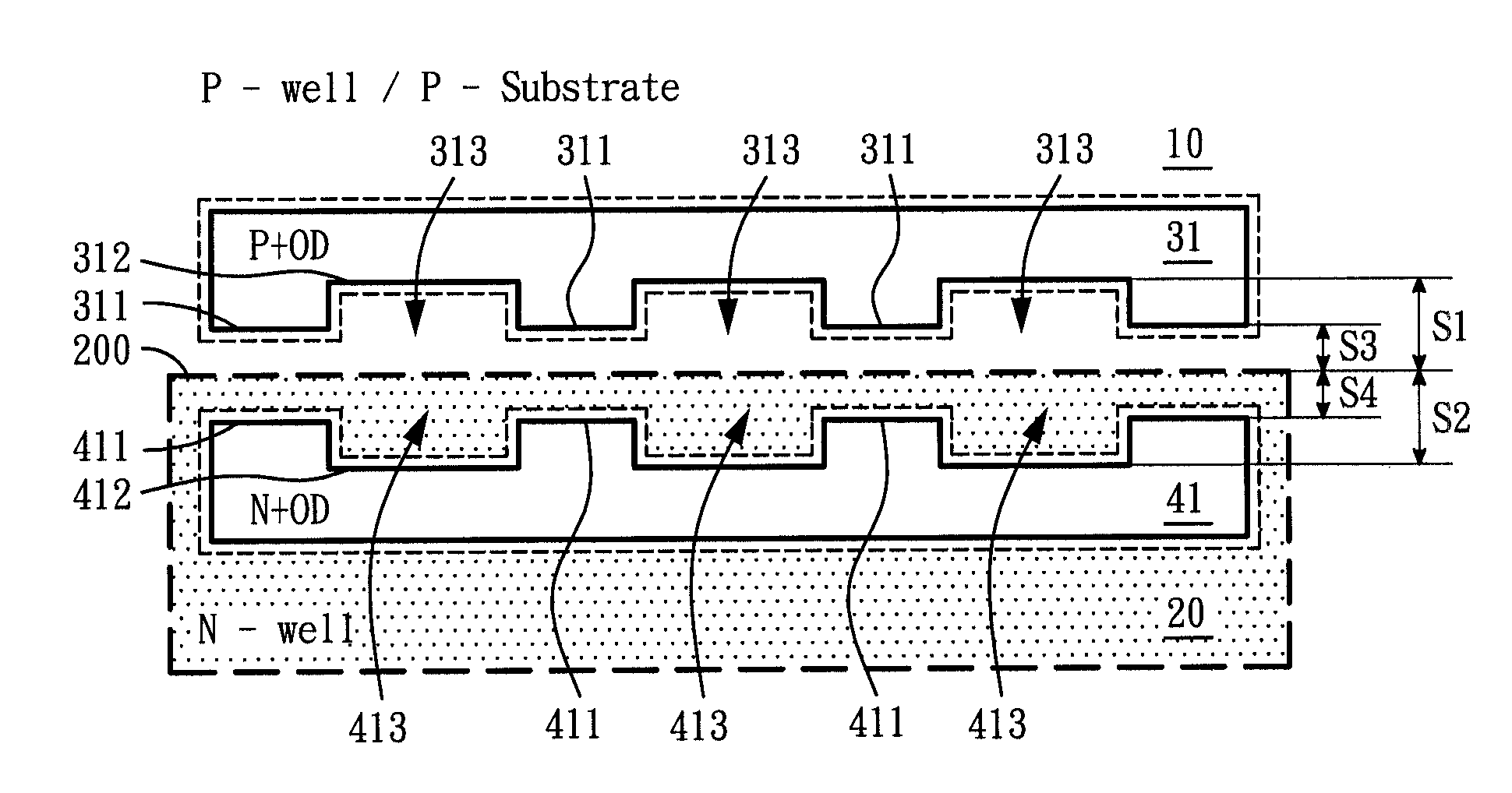
[0026]In FIG. 3, a first well 10 of a first type is formed on a semiconductor substrate. A second well 20 of a second type, alongside the first well 10, is also formed. According to one embodiment, a first heavily doped region 31 and a second heavily doped region 41 are formed in the wells 10 and 20. Particularly, the first heavily doped region 31 of the first type is formed in the first well 10. The second heavily doped region 41 of the second type is formed in the second well 20. In one embodiment, the first heavily doped region 31 comprises a p+ type region formed in the p-well 10 having a battlement layout pattern along the boundary between the first and the second wells. The second heavily doped region 41 comprises an n+ type region formed in the n-well 20 having a battlement layout pattern along the boundary between the first and the second wells. In one embodiment, those concave shape regions in the second heavily doped region 41 are opposite to those concave shape regions in...

second embodiment

[0028]In FIG. 4, a first well 10 of a first type is formed on a semiconductor substrate. A second well 20 of a second type, alongside the first well 10, is also formed. According to one embodiment, a first heavily doped regions 30 and a second heavily doped region 41 are formed in the wells 10 and 20. Particularly, the first heavily doped region 30 of the first type is formed in the first well 10. The second heavily doped region 41 of the second type is formed in the second well 20. In one embodiment, the first heavily doped region 30 comprises a p+ type region formed in the p-well 10. The second heavily doped region 41 comprises an n+ type region formed in the n-well 20 having a battlement layout pattern along the boundary between the first and the second wells.

[0029]In FIG. 3, a first well 10 of a first type is formed on a semiconductor substrate. A second well 20 of a second type, alongside the first well 10, is also formed. According to one embodiment, a first heavily doped regi...

third embodiment

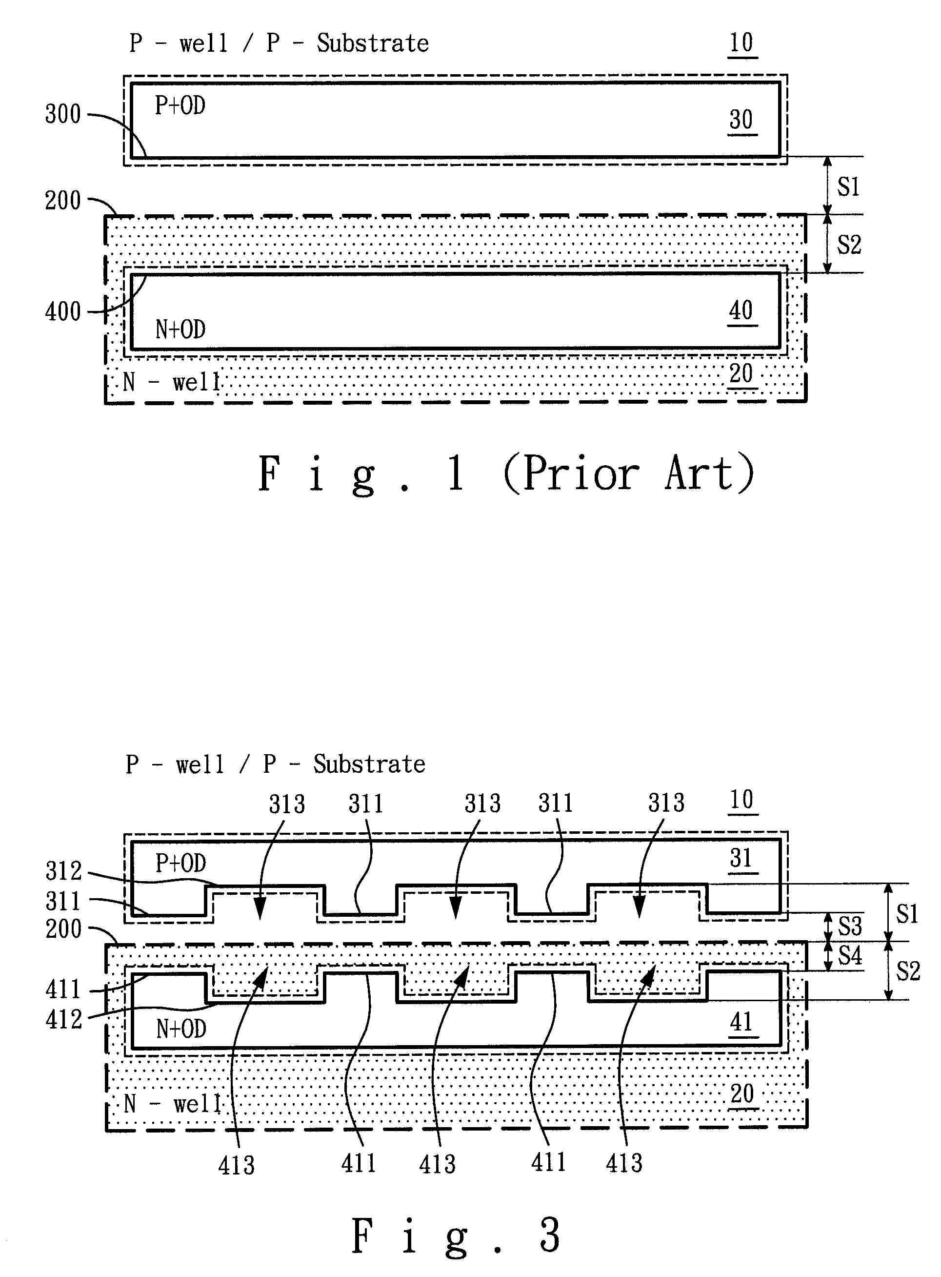
[0030]Furthermore, a distance between each ridge 311 of the first heavily doped region 31 and the edge 200 of the second well 20 facing the ridges 311 is S3. A distance between each ridge 411 of the second heavily doped region 41 and the edge 200 of the second well 20 is S4. A distance between a bottom 312 of each recessed concave region 313 and the edge 200 of the second well 20 is S1. A distance between a bottom 412 of each recessed concave region 413 and the edge 200 of the second well 20 is S2. The distances S3 and S4 are arranged to be less than what is typically required by the layout rule of internal circuit. If the DC power noise occurs, the abrupt power noise pulse will breakdown the p-n well junction of the ESD circuit device and discharge ESD current to protect the internal circuit. However, S3 and S4 may not be curtailed unlimitedly. S3 and S4 have to maintain a certain length to ensure the breakdown voltage of the p-n well junction of the ESD circuit device to be greate...


PUM


Abstract

An improved layout pattern for electrostatic discharge protection is disclosed. A first heavily doped region of a first type is formed in a well of said first type. A second heavily doped region of a second type is formed in a well of said second type. A battlement layout pattern of said first heavily doped region is formed along the boundary of said first heavily doped region and said second heavily doped region. A battlement layout pattern of said second heavily doped region is formed along the boundary of said first heavily doped region and said second heavily doped region. By adjusting a distance between the battlement layout pattern of a heavily doped region and a edge of well of said second type, i.e. n-well, a first distance will be shorter than what is typically required by the layout rules of internal circuit; and a second distance will be longer than the first distance to ensure that the I / O device have a better ESD protection capability. Accordingly, by properly adjusting the breakdown voltage of ESD device within I / O circuit, i.e. adjusting the distance between the edge of n-well and the battlement layout pattern of heavily doped regions, it will help to reduce the chip area and improve the ESD reliability.

Description

BACKGROUND[0001]1. Field of the Invention[0002]The present invention relates generally to electrostatic discharge protection for semiconductor integrated circuitry and more particularly to an improved layout structure / pattern for electrostatic discharge protection[0003]2. Background of the Invention[0004]Static electricity has been an industrial problem for centuries. Since ancient time, people employed basic grounding and flame ionization techniques to dissipate static electricity and to refrain from ignition to combustible objects. The age of electronics brought with it new problems associated with static electricity and electrostatic discharge (“ESD”). And as electronic devices become faster and smaller, their sensitivity to ESD also increases.[0005]Static electricity is defined as an electrical charge caused by an imbalance of electrons on the surface of a material. ESD is defined as the transfer of charge between bodies at different electrical potentials. ESD can change the ele...

Claims


Application Information

Patent Timeline
Patent Type & Authority Patents(United States)
IPC IPC(8): H01L23/62
CPCH01L27/0255H01L29/0692
Inventor CHEN, TUNG-YANG
Owner HIMAX TECH LTD
Why Eureka
Try Eureka