

Electromagnetic digitizer sensor array structure
a technology of electromagnetic digitizer and sensor array, which is applied in the direction of photometry using electric radiation detectors, optical radiation measurement, instruments, etc., can solve the problems of relatively large physical size of printed circuit technology, low resolution, and large physical dimension of sensor array, and achieve the effect of enhancing the sensitivity of the sensor array
- Summary
- Abstract
- Description
- Claims
- Application Information
AI Technical Summary
Benefits of technology
Problems solved by technology
Method used
Image

Examples
Embodiment Construction
The present description is of the best presently contemplated mode of carrying out the invention. This description is made for the purpose of illustrating the general principles of the invention and should not be taken in a limiting sense. The scope of the invention is best determined by reference to the appended claims. This invention has been described herein in reference to various embodiments and drawings. It will be appreciated by those skilled in the art that variations and improvements may be accomplished in view of these teachings without deviating from the scope and spirit of the invention.
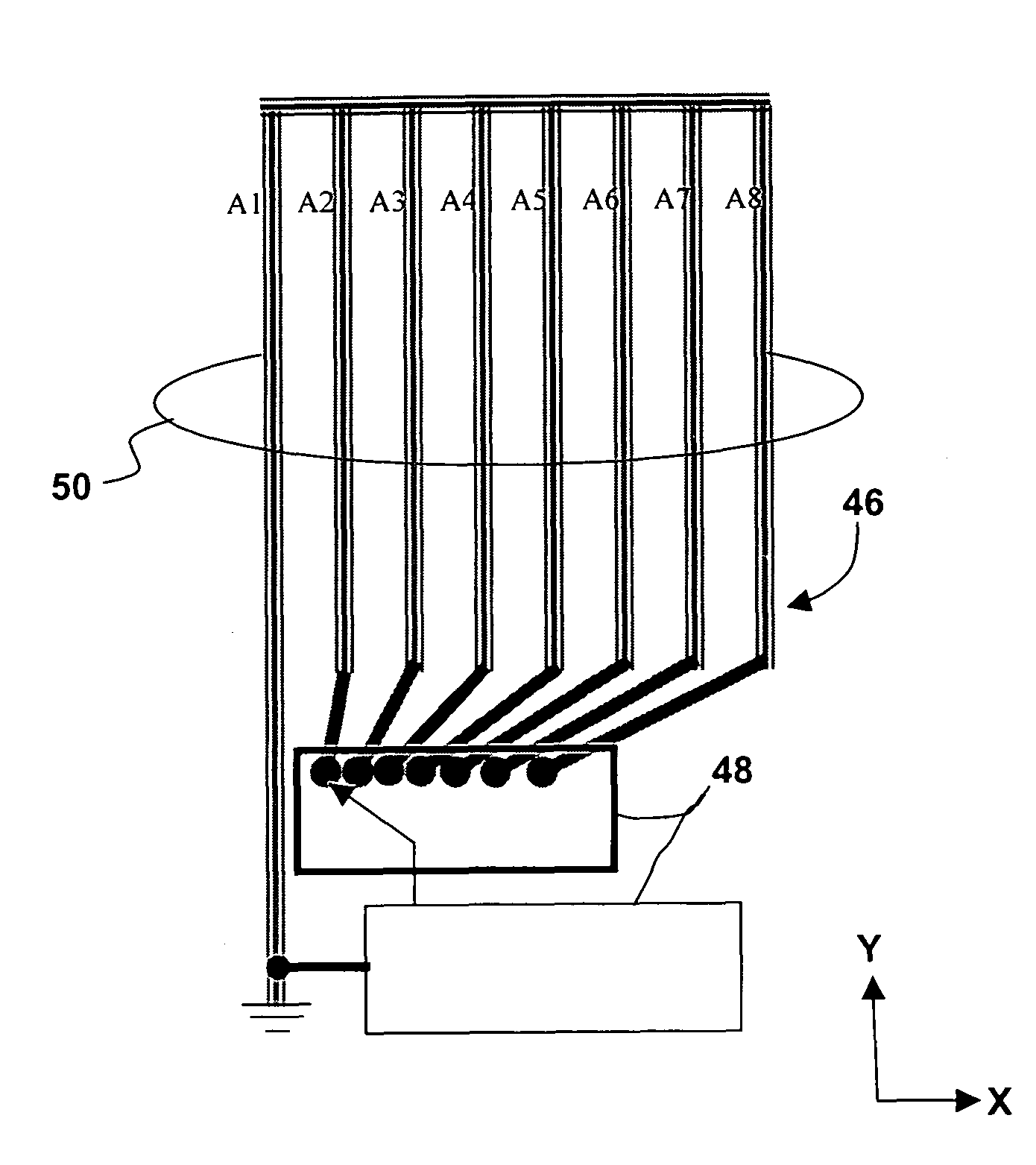
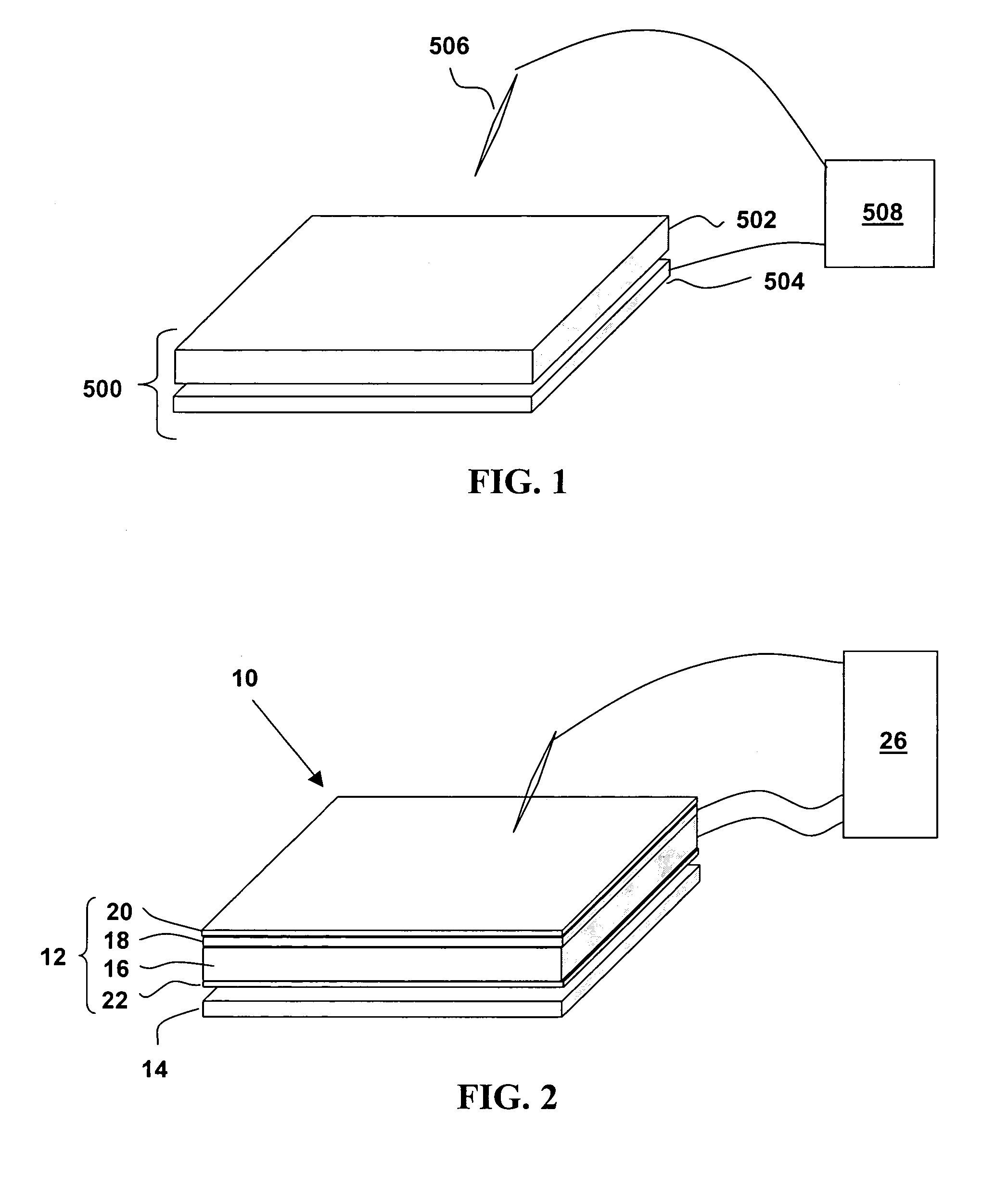
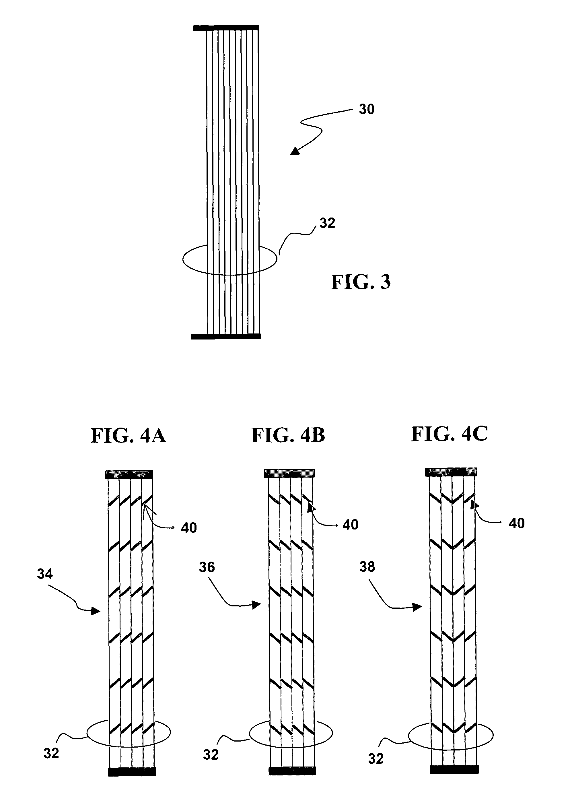
The present invention overcomes the drawback of the prior art electromagnetic digitizers by providing a novel structure for the sensor segments in the sensor array. The sensor segment structure may be advantageously adapted for integration into the display module of a display device. By way of illustration and not limitation, the present invention will be described in connection with a fl...
PUM
 Abstract
Description
Claims
Application Information