
Reduction of fragmentation in nonvolatile memory using alternate address mapping

a nonvolatile memory and address mapping technology, applied in the direction of memory address formation, micro-instruction address formation, allocation/relocation, etc., can solve the problems of deteriorating write performance, large number of physical blocks, and long time-consuming write processing, so as to reduce the number of copying and erasing processing and improve the efficiency of writing processing

Active Publication Date: 2011-01-25
PANASONIC CORP
View PDF16 Cites 25 Cited by
  • Summary
  • Abstract
  • Description
  • Claims
  • Application Information

AI Technical Summary

Benefits of technology

[0014]The present invention is made to solve the above-mentioned problems, and it is an object of the present invention to provide a nonvolatile storage device that does not depend on the access method of the host and can shorten the time required for write processing.
[0017]According to the present invention, when data is written in a certain logical address in a nonvolatile memory and then another data is re-written in the same logical address, duplication (redundant) writing is allowed, which writes the another data newly in a physical region different from the physical region in which the data is written previously while holding and not erasing the data previously written in the physical address. This can reduce the number of copying and erasing processing due to data update, which is specific property of a nonvolatile memory, and improve efficiency in writing processing. Furthermore, a write mode is selectively switched in accordance with change in a write address, and thus the write processing can be implemented in more optimum method without depending on the type (sequential access or random access) of write requests from the host.

Problems solved by technology

This difference gives rise to fragmentation of the file written in the memory card, resulting in deteriorated write performance.
In the write method of the conventional nonvolatile memory under the condition where fragmentation occurs, as described above, there exists problems in that it takes a long time to perform write processing, and that a large number of physical blocks which carry out write and erase operations are required.

Method used


Image

  • Reduction of fragmentation in nonvolatile memory using alternate address mapping
  • Reduction of fragmentation in nonvolatile memory using alternate address mapping
  • Reduction of fragmentation in nonvolatile memory using alternate address mapping

Examples


example 1

Example of Sequential Write Mode

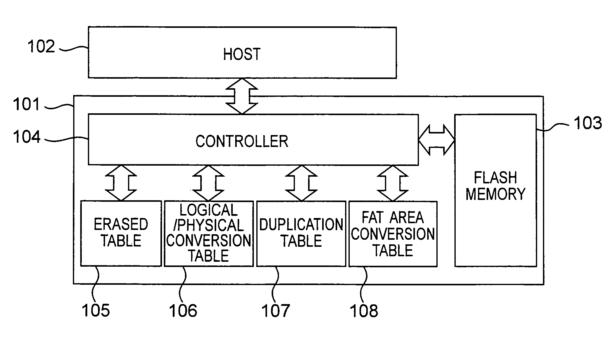
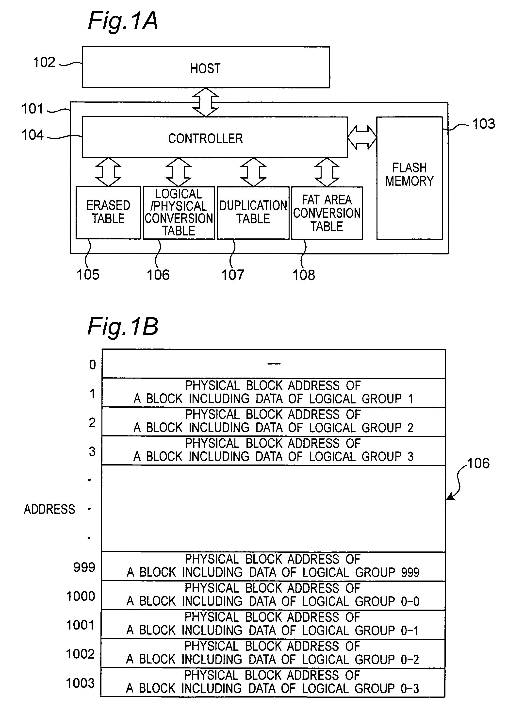
[0213]Referring now to FIG. 25 through FIG. 31, an example from new write mode to sequential write mode will be explained. In FIG. 25, when data writing is requested newly from the host 102 to regions of logical block 0x0010, logical sectors 0x0020 through 0x003F, the new writing (S24) takes place in the case of no registration in the duplication information (S12), and data is written to the physical block 100 which is an erased block.

[0214]Under the above-mentioned situation, the duplication information 107b of the duplication table 107 is set as follows. The value of “logical block address” is set to logical address 0x0010 designated by the host 102. The value of “destination physical block address is set to 0x0000 which corresponds to the logical block address of 0x0010 in the logical / physical conversion table. The value of “destination physical block address” is set to 0x0100 indicating the block address of the physical block 100 to which the data...

example 2

Example of Overwrite Mode

[0220]Referring now to FIG. 32 through FIG. 34, description will be made on an example in the case of overwrite mode from new write mode. In FIG. 32, when a request is made by the host 102 to newly write data to regions of logical block 0x0010 and logical sectors 0x00E0 through 0x00FF, the data is written to the physical block 100 which is the erased block.

[0221]Under the above-mentioned situation, the duplication information 107b of the duplication table 107 is set as follows. “logical block address” is set to the logical address 0x0010 designated from the host 102. “destination physical block address” is set to 0x0000 which is a value that corresponds to the logical block address 0x0010 in the logical / physical conversion table. “destination physical block address” is set to 0x0100 which indicates the block address of the physical block 100 to which the data is to be written. “destination top page logical address” is set to 0x00E0 which is a value of the he...

example 3

Aggregation of Overwritten Blocks

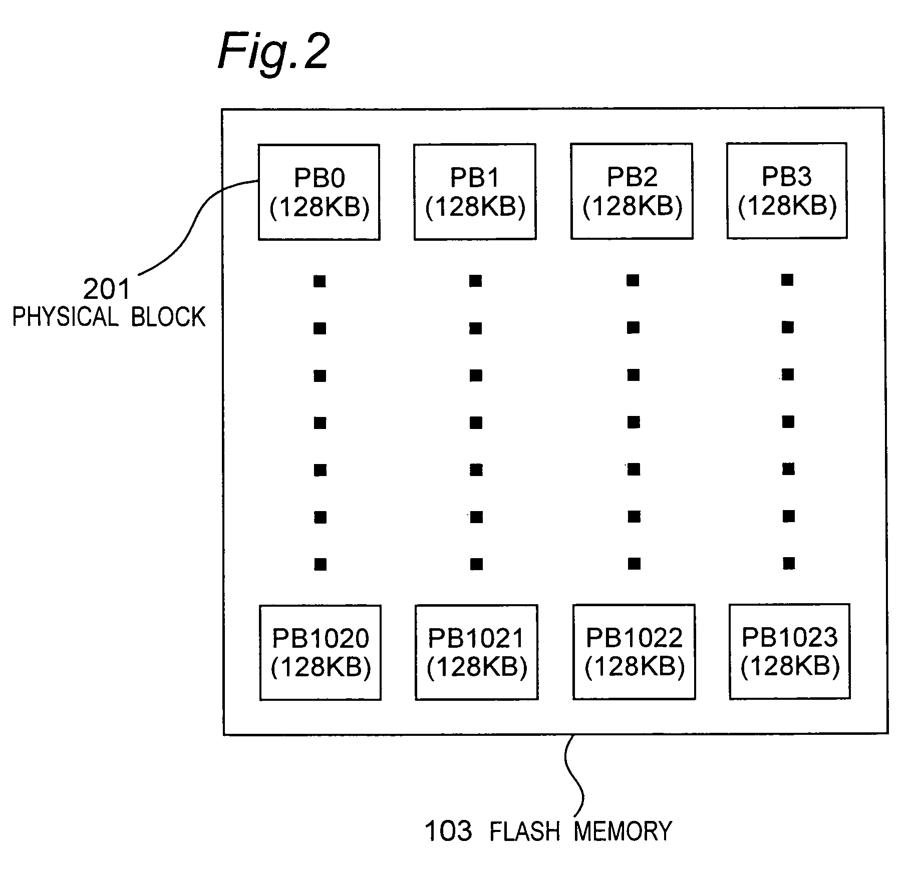
[0224]Referring now to FIG. 35 and FIG. 36, description will be made on the example of aggregation processing of overwritten blocks. As shown in FIG. 35, the data lastly overwritten in the physical block 100 is copied to the erased physical block 101. In the physical block 101, it is necessary to write the data read out from the “source physical block” the of duplication information 107b in the remaining region (pages 8 through 3F), but in this example, since 0x0000 which indicates an invalid value is stored in the “source physical block” of the duplication information 107b, a predetermined data (FF) is written.

[0225]Thereafter, as shown in FIG. 36, the physical block 100 is erased. Along with this, the duplication information concerning the physical block 100 is initialized, and at the same time, a physical block 101 is registered to the logical / physical conversion table 106.


PUM


Abstract

A nonvolatile storage device can read and write data by receiving a logical address from a host. The nonvolatile storage device includes: a nonvolatile memory writing and reading data based on a physical address; a logical / physical conversion table storing information on correspondence between the logical address and the physical address for each of a plurality of data management units; a duplication table storing information on correspondence between the logical address and the physical address of data arranged over a plurality of areas in a duplicate (redundant) manner in the nonvolatile memory and having a size smaller than a size of a data management unit; and a controller controlling an operation of the nonvolatile storage device. The controller permits duplicate (redundant) writing of data having a same logical address as the data (which has been written in one data management unit in another data management unit), and the controller performs a plurality of write modes for the duplicate (redundant) writing, and selectively switches between the write modes according to situation of a logical address change designated by the host.

Description

BACKGROUND OF THE INVENTION[0001]1. Field of Invention[0002]The present invention relates to a storage device using a nonvolatile memory such as a flash memory, etc. and a writing method thereof.[0003]2. Description of the Related Art[0004]In recent years, memory cards loaded with a nonvolatile memory as storage media of digital cameras and cellular phones have expanded in their market. As the memory card capacity increases, the applications are expanded from recording with small capacity of data files, still images, and others, to recording with large-capacity required for moving pictures. Consequently, various developments have been made with respect to a recording medium including a nonvolatile memory (for example, patent documents 1 through 4).[0005]In recent years, in a NAND type flash memory primarily used for nonvolatile memory of memory cards, a physical block size which is a data erase unit increases from 16 kB (mainly in a flash memory of 128 MB or smaller) to 128 kB (main...

Claims


Application Information

Patent Timeline
Patent Type & Authority Patents(United States)
IPC IPC(8): G06F12/10G06F3/06G06F3/08G06F12/00G06F12/02
CPCG06F3/0607G06F3/0611G06F3/064G06F3/0643G06F3/0679G06F11/2069G06F11/2087G06F12/0246G06F2212/7201G06F2212/7202G06F3/08G06F12/00G06F12/02
Inventor HONDA, TOSHIYUKI
Owner PANASONIC CORP
Learn More